- 您现在的位置:买卖IC网 > PDF目录295111 > AT40KEL040KZ1SB (ATMEL CORP) FPGA, 2304 CLBS, 50000 GATES, PQFP256 PDF资料下载
参数资料
| 型号: | AT40KEL040KZ1SB |
| 厂商: | ATMEL CORP |
| 元件分类: | FPGA |
| 英文描述: | FPGA, 2304 CLBS, 50000 GATES, PQFP256 |
| 封装: | MQFP-256 |
| 文件页数: | 42/42页 |
| 文件大小: | 670K |
| 代理商: | AT40KEL040KZ1SB |
第1页第2页第3页第4页第5页第6页第7页第8页第9页第10页第11页第12页第13页第14页第15页第16页第17页第18页第19页第20页第21页第22页第23页第24页第25页第26页第27页第28页第29页第30页第31页第32页第33页第34页第35页第36页第37页第38页第39页第40页第41页当前第42页
9
AT40KEL040
4155G–AERO–05/05
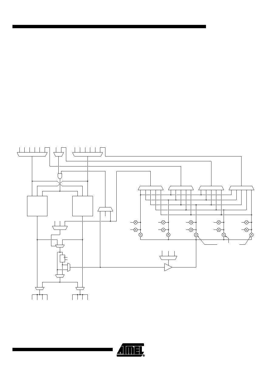
The Cell
Figure 5 depicts the AT40KEL040 cell. Configuration bits for separate muxes and pass
gates are independent. All permutations of programmable muxes and pass gates are
legal. Vn (V1 -V5) is connected to the vertical local bus in plane n. Hn (H1 -H5) is con-
nected to the horizontal local bus in plane n. A local/local turn in plane n is achieved by
turning on the two pass gates connected to V
n and Hn. Pass gates are opened to let sig-
nals into the cell from a local bus or to drive a signal out onto a local bus. Signals coming
into the logic cell on one local bus plane can be switched onto another plane by opening
two of the pass gates. This allows bus signals to switch planes to achieve greater
routability. Up to five simultaneous local/local turns are possible.
The AT40KEL040 FPGA core cell is a highly configurable logic block based around two
3-input LUTs (8 x 1 ROM), which can be combined to produce one 4-input LUT. This
means that any core cell can implement two functions of 3 inputs or one function of 4
inputs. There is a Set/Reset D flip-flop in every cell, the output of which may be tri-stated
and fed back internally within the core cell. There is also a 2-to-1 multiplexer in every
cell, and an upstream AND gate in the “front end” of the cell. This AND gate is an impor-
tant feature in the implementation of efficient array multipliers.
Figure 5. The Cell
With this functionality in each core cell, the core cell can be configured in several
“modes”. The core cell flexibility makes the AT40KEL040 architecture well suited to
most digital design application areas (see Figure 6).
OUT
RESET/SET
CLOCK
FB
10
Z
D
Q
"1" NW NE SE SW
"1"
"0"
XW
Y
X
ZW
Y
"1"
N
E
S
W
8X1 LUT
X
Y
NW NE SE SW
N
E
S
W
V1
H1
V2
H2
V3
H3
V4
H4
V5
H5
"1" OEH OEV
L
Pass gates
X = Diagonal Direct connect or Bus
Y = Orthogonal Direct Connector Bus
W = Bus Connection
Z = Bus Connection
FB = Internal Feed back
相关PDF资料 |
PDF描述 |
|---|---|
| AT89C2051-12SCT/R | 8-BIT, FLASH, 12 MHz, MICROCONTROLLER, PDSO20 |
| AT89C51-24JCT/R | 8-BIT, FLASH, 24 MHz, MICROCONTROLLER, PQCC44 |
| AT89C55-12JA | 8-BIT, FLASH, 12 MHz, MICROCONTROLLER, PQCC44 |
| AT90-1263TR | 0 MHz - 3000 MHz RF/MICROWAVE VARIABLE ATTENUATOR, 3.8 dB INSERTION LOSS-MAX |
| AT90S1200A-4YI | 8-BIT, FLASH, 4 MHz, RISC MICROCONTROLLER, PDSO20 |
相关代理商/技术参数 |
参数描述 |
|---|---|
| AT40K-FFT | 制造商:未知厂家 制造商全称:未知厂家 功能描述:AT40K-FFT [Updated 8/98. 8 Pages] Fast fourier transform Intellectual Property Core for AT40K FPGAs |
| AT40KFL040 | 制造商:ATMEL 制造商全称:ATMEL Corporation 功能描述:Rad Hard Reprogrammable FPGAs with FreeRAM |
| AT40KFL040KW1-E | 制造商:ATMEL 制造商全称:ATMEL Corporation 功能描述:Rad Hard Reprogrammable FPGAs with FreeRAM |
| AT40KFL040KW1-SCC | 制造商:ATMEL 制造商全称:ATMEL Corporation 功能描述:Rad Hard Reprogrammable FPGAs with FreeRAM |
| AT40KFL040KZ1-E | 制造商:ATMEL 制造商全称:ATMEL Corporation 功能描述:Rad Hard Reprogrammable FPGAs with FreeRAM |
发布紧急采购,3分钟左右您将得到回复。