- 您现在的位置:买卖IC网 > PDF目录381460 > AT49LV020 (Atmel Corp.) 256K x 8 Single 2.7-volt Battery-Voltage Flash Memory(256K x 8单电源2.7V Battery-Voltage技术闪速存储器) PDF资料下载
参数资料
| 型号: | AT49LV020 |
| 厂商: | Atmel Corp. |
| 英文描述: | 256K x 8 Single 2.7-volt Battery-Voltage Flash Memory(256K x 8单电源2.7V Battery-Voltage技术闪速存储器) |
| 中文描述: | 256K × 8单2.7伏电池电压快闪记忆体(256K × 8单电源为2.7V电池电压技术闪速存储器) |
| 文件页数: | 2/13页 |
| 文件大小: | 212K |
| 代理商: | AT49LV020 |
AT49BV/LV020
2
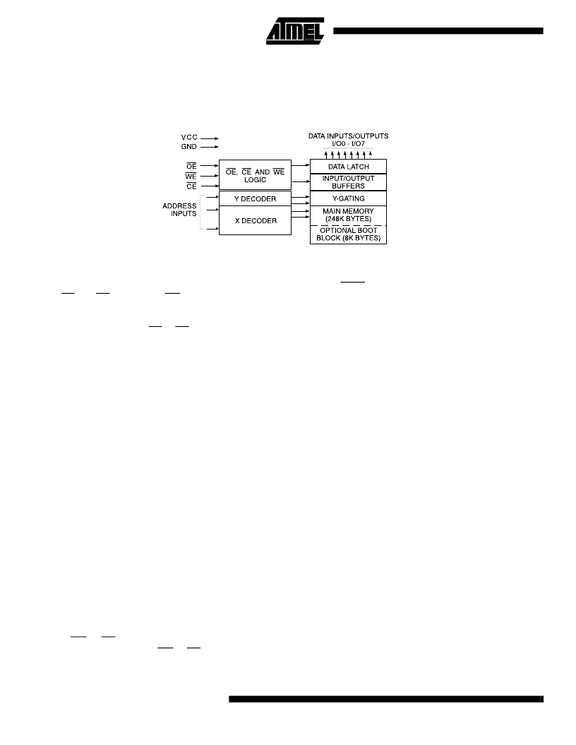
The optional 8K bytes boot block section includes a repro-
gramming write lock out feature to provide data integrity.
The boot sector is designed to contain user secure code,
and when the feature is enabled, the boot sector is perma-
nently protected from being reprogrammed.
Block Diagram
Device Operation
READ:
The AT49BV/LV020 is accessed like an EPROM.
When CE and OE are low and WE is high, the data stored
at the memory location determined by the address pins is
asserted on the outputs. The outputs are put in the high
impedance state whenever CE or OE is high. This dual-line
control gives designers flexibility in preventing bus conten-
tion.
ERASURE:
Before a byte can be reprogrammed, the 256K
bytes memory array (or 248K bytes if the boot block fea-
tured is used) must be erased. The erased state of the
memory bits is a logical
“
1
”
. The entire device can be
erased at one time by using a 6-byte software code. The
software chip erase code consists of 6-byte load com-
mands to specific address locations with a specific data
pattern (please refer to the Chip Erase Cycle Waveforms).
After the software chip erase has been initiated, the device
will internally time the erase operation so that no external
clocks are required. The maximum time needed to erase
the whole chip is t
EC
. If the boot block lockout feature has
been enabled, the data in the boot sector will not be
erased.
BYTE PROGRAMMING:
Once the memory array is
erased, the device is programmed (to a logical
“
0
”
) on a
byte-by-byte basis. Please note that a data
“
0
”
cannot be
programmed back to a
“
1
”
; only erase operations can con-
vert
“
0
”
s to
“
1
”
s. Programming is accomplished via the
internal device command register and is a 4 bus cycle
operation (please refer to the Command Definitions table).
The device will automatically generate the required internal
program pulses.
The program cycle has addresses latched on the falling
edge of WE or CE, whichever occurs last, and the data
latched on the rising edge of WE or CE, whichever occurs
first. Programming is completed after the specified t
BP
cycle
time. The DATA polling feature may also be used to indi-
cate the end of a program cycle.
BOOT BLOCK PROGRAMMING LOCKOUT:
The device
has one designated block that has a programming lockout
feature. This feature prevents programming of data in the
designated block once the feature has been enabled. The
size of the block is 8K bytes. This block, referred to as the
boot block, can contain secure code that is used to bring up
the system. Enabling the lockout feature will allow the boot
code to stay in the device while data in the rest of the
device is updated. This feature does not have to be acti-
vated; the boot block's usage as a write protected region is
optional to the user. The address range of the boot block is
00000H to 01FFFH.
Once the feature is enabled, the data in the boot block can
no longer be erased or programmed. Data in the main
memory block can still be changed through the regular pro-
gramming method. To activate the lockout feature, a series
of six program commands to specific addresses with spe-
cific data must be performed. Please refer to the Command
Definitions table.
BOOT BLOCK LOCKOUT DETECTION:
A software
method is available to determine if programming of the boot
block section is locked out. When the device is in the soft-
ware product identification mode (see Software Product
Identification Entry and Exit sections) a read from address
location 00002H will show if programming the boot block is
locked out. If the data on I/O0 is low, the boot block can be
programmed; if the data on I/O0 is high, the program lock-
out feature has been activated and the block cannot be
programmed. The software product identification code
should be used to return to standard operation.
PRODUCT IDENTIFICATION:
The product identification
mode identifies the device and manufacturer as Atmel. It
00000
01FFF
02000
3FFFF
相关PDF资料 |
PDF描述 |
|---|---|
| AT49BV040A | 4-megabit (512K x 8) Single 2.7-volt Battery-Voltage⑩ Flash Memory |
| AT49BV040A-70JI | LM4665 Boomer ® Audio Power Amplifier Series Filterless High Efficiency 1W Switching Audio Amplifier; Package: MICRO SMD; No of Pins: 9 |
| AT49BV040A-70TI | LM4665 Boomer ® Audio Power Amplifier Series Filterless High Efficiency 1W Switching Audio Amplifier; Package: MICRO SMD; No of Pins: 9 |
| AT49BV040A-70VI | LM4665 Boomer ® Audio Power Amplifier Series Filterless High Efficiency 1W Switching Audio Amplifier; Package: LLP; No of Pins: 10 |
| AT49BV040T | 512K x 8 Single 2.7-volt Battery-Voltage Flash Memory(512K x 8单电源2.7V Battery-Voltage技术闪速存储器) |
相关代理商/技术参数 |
参数描述 |
|---|---|
| AT49LV040-12JC | 功能描述:闪存 4M bit RoHS:否 制造商:ON Semiconductor 数据总线宽度:1 bit 存储类型:Flash 存储容量:2 MB 结构:256 K x 8 定时类型: 接口类型:SPI 访问时间: 电源电压-最大:3.6 V 电源电压-最小:2.3 V 最大工作电流:15 mA 工作温度:- 40 C to + 85 C 安装风格:SMD/SMT 封装 / 箱体: 封装:Reel |
| AT49LV040-12JI | 功能描述:闪存 4M bit RoHS:否 制造商:ON Semiconductor 数据总线宽度:1 bit 存储类型:Flash 存储容量:2 MB 结构:256 K x 8 定时类型: 接口类型:SPI 访问时间: 电源电压-最大:3.6 V 电源电压-最小:2.3 V 最大工作电流:15 mA 工作温度:- 40 C to + 85 C 安装风格:SMD/SMT 封装 / 箱体: 封装:Reel |
| AT49LV040-12TC | 功能描述:闪存 4M bit RoHS:否 制造商:ON Semiconductor 数据总线宽度:1 bit 存储类型:Flash 存储容量:2 MB 结构:256 K x 8 定时类型: 接口类型:SPI 访问时间: 电源电压-最大:3.6 V 电源电压-最小:2.3 V 最大工作电流:15 mA 工作温度:- 40 C to + 85 C 安装风格:SMD/SMT 封装 / 箱体: 封装:Reel |
| AT49LV040-12TI | 功能描述:IC FLASH 4MBIT 120NS 32TSOP RoHS:否 类别:集成电路 (IC) >> 存储器 系列:- 标准包装:378 系列:- 格式 - 存储器:闪存 存储器类型:FLASH 存储容量:8M(1M x 8,512K x 16) 速度:110ns 接口:并联 电源电压:2.7 V ~ 3.6 V 工作温度:-40°C ~ 85°C 封装/外壳:48-CBGA 供应商设备封装:48-CBGA(7x7) 包装:托盘 |
| AT49LV040-12VC | 功能描述:闪存 4M bit RoHS:否 制造商:ON Semiconductor 数据总线宽度:1 bit 存储类型:Flash 存储容量:2 MB 结构:256 K x 8 定时类型: 接口类型:SPI 访问时间: 电源电压-最大:3.6 V 电源电压-最小:2.3 V 最大工作电流:15 mA 工作温度:- 40 C to + 85 C 安装风格:SMD/SMT 封装 / 箱体: 封装:Reel |
发布紧急采购,3分钟左右您将得到回复。