- 您现在的位置:买卖IC网 > PDF目录11806 > AT89C51CC01UA-RLRUM (Atmel)IC 8051 MCU 32K FLASH 44-VQFP PDF资料下载
参数资料
| 型号: | AT89C51CC01UA-RLRUM |
| 厂商: | Atmel |
| 文件页数: | 100/123页 |
| 文件大小: | 0K |
| 描述: | IC 8051 MCU 32K FLASH 44-VQFP |
| 产品培训模块: | MCU Product Line Introduction |
| 标准包装: | 1,500 |
| 系列: | AT89C CAN |
| 核心处理器: | 8051 |
| 芯体尺寸: | 8-位 |
| 速度: | 40MHz |
| 连通性: | CAN,UART/USART |
| 外围设备: | POR,PWM,WDT |
| 输入/输出数: | 34 |
| 程序存储器容量: | 32KB(32K x 8) |
| 程序存储器类型: | 闪存 |
| EEPROM 大小: | 2K x 8 |
| RAM 容量: | 1.25K x 8 |
| 电压 - 电源 (Vcc/Vdd): | 3 V ~ 5.5 V |
| 数据转换器: | A/D 8x10b |
| 振荡器型: | 外部 |
| 工作温度: | -40°C ~ 85°C |
| 封装/外壳: | 44-LQFP |
| 包装: | 标准包装 |
| 配用: | AT89OCD-01-ND - USB EMULATOR FOR AT8XC51 MCU |
| 其它名称: | AT89C51CC01UA-RLRUMDKR |
第1页第2页第3页第4页第5页第6页第7页第8页第9页第10页第11页第12页第13页第14页第15页第16页第17页第18页第19页第20页第21页第22页第23页第24页第25页第26页第27页第28页第29页第30页第31页第32页第33页第34页第35页第36页第37页第38页第39页第40页第41页第42页第43页第44页第45页第46页第47页第48页第49页第50页第51页第52页第53页第54页第55页第56页第57页第58页第59页第60页第61页第62页第63页第64页第65页第66页第67页第68页第69页第70页第71页第72页第73页第74页第75页第76页第77页第78页第79页第80页第81页第82页第83页第84页第85页第86页第87页第88页第89页第90页第91页第92页第93页第94页第95页第96页第97页第98页第99页当前第100页第101页第102页第103页第104页第105页第106页第107页第108页第109页第110页第111页第112页第113页第114页第115页第116页第117页第118页第119页第120页第121页第122页第123页
38
A/T89C51CC01
4129N–CAN–03/08
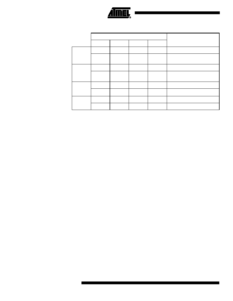
Table 26. Programming Spaces
Notes:
1. The sequence 5xh and Axh must be executing without instructions between them
otherwise the programming is aborted.
2. Interrupts that may occur during programming time must be disabled to avoid any
spurious exit of the programming mode.
Status of the Flash Memory
The bit FBUSY in FCON register is used to indicate the status of programming.
FBUSY is set when programming is in progress.
Selecting FM1
The bit ENBOOT in AUXR1 register is used to map FM1 from F800h to FFFFh.
Loading the Column Latches
Any number of data from 1 Byte to 128 Bytes can be loaded in the column latches. This
provides the capability to program the whole memory by byte, by page or by any number
of Bytes in a page.
When programming is launched, an automatic erase of the locations loaded in the col-
umn latches is first performed, then programming is effectively done. Thus no page or
block erase is needed and only the loaded data are programmed in the corresponding
page.
The following procedure is used to load the column latches and is summarized in
Save then disable interrupt and map the column latch space by setting FPS bit.
Load the DPTR with the address to load.
Load Accumulator register with the data to load.
Execute the MOVX @DPTR, A instruction.
If needed loop the three last instructions until the page is completely loaded.
Unmap the column latch and Restore Interrupt
Write to FCON
Operation
FPL3:0
FPS
FMOD1
FMOD0
User
5
X
0
No action
A
X
0
Write the column latches in user
space
Extra Row
5
X
0
1
No action
A
X
0
1
Write the column latches in extra row
space
Hardware
Security
Byte
5
X
1
0
No action
A
X
1
0
Write the fuse bits space
Reserved
5
X
1
No action
A
X
1
No action
相关PDF资料 |
PDF描述 |
|---|---|
| VE-B5R-IW-F4 | CONVERTER MOD DC/DC 7.5V 100W |
| VE-B5R-IW-F3 | CONVERTER MOD DC/DC 7.5V 100W |
| VE-B5R-IW-F2 | CONVERTER MOD DC/DC 7.5V 100W |
| VE-B5P-IX-F3 | CONVERTER MOD DC/DC 13.8V 75W |
| VE-B5P-IX-F1 | CONVERTER MOD DC/DC 13.8V 75W |
相关代理商/技术参数 |
参数描述 |
|---|---|
| AT89C51CC01UA-RLTUM | 功能描述:8位微控制器 -MCU CAN Bootloader UART RoHS:否 制造商:Silicon Labs 核心:8051 处理器系列:C8051F39x 数据总线宽度:8 bit 最大时钟频率:50 MHz 程序存储器大小:16 KB 数据 RAM 大小:1 KB 片上 ADC:Yes 工作电源电压:1.8 V to 3.6 V 工作温度范围:- 40 C to + 105 C 封装 / 箱体:QFN-20 安装风格:SMD/SMT |
| AT89C51CC01UA-SLSUM | 功能描述:8位微控制器 -MCU CAN-STICK Bootloader UART IND RoHS:否 制造商:Silicon Labs 核心:8051 处理器系列:C8051F39x 数据总线宽度:8 bit 最大时钟频率:50 MHz 程序存储器大小:16 KB 数据 RAM 大小:1 KB 片上 ADC:Yes 工作电源电压:1.8 V to 3.6 V 工作温度范围:- 40 C to + 105 C 封装 / 箱体:QFN-20 安装风格:SMD/SMT |
| AT89C51CC01UU-RLTUM | 功能描述:8位微控制器 -MCU Microcontroller RoHS:否 制造商:Silicon Labs 核心:8051 处理器系列:C8051F39x 数据总线宽度:8 bit 最大时钟频率:50 MHz 程序存储器大小:16 KB 数据 RAM 大小:1 KB 片上 ADC:Yes 工作电源电压:1.8 V to 3.6 V 工作温度范围:- 40 C to + 105 C 封装 / 箱体:QFN-20 安装风格:SMD/SMT |
| AT89C51CC01UU-SLSUM | 功能描述:8位微控制器 -MCU Microcontroller RoHS:否 制造商:Silicon Labs 核心:8051 处理器系列:C8051F39x 数据总线宽度:8 bit 最大时钟频率:50 MHz 程序存储器大小:16 KB 数据 RAM 大小:1 KB 片上 ADC:Yes 工作电源电压:1.8 V to 3.6 V 工作温度范围:- 40 C to + 105 C 封装 / 箱体:QFN-20 安装风格:SMD/SMT |
| AT89C51CC02 | 制造商:ATMEL 制造商全称:ATMEL Corporation 功能描述:Enhanced 8-bit Microcontroller with CAN Controller and Flash |
发布紧急采购,3分钟左右您将得到回复。