- 您现在的位置:买卖IC网 > PDF目录11806 > AT89C51CC01UA-RLRUM (Atmel)IC 8051 MCU 32K FLASH 44-VQFP PDF资料下载
参数资料
| 型号: | AT89C51CC01UA-RLRUM |
| 厂商: | Atmel |
| 文件页数: | 113/123页 |
| 文件大小: | 0K |
| 描述: | IC 8051 MCU 32K FLASH 44-VQFP |
| 产品培训模块: | MCU Product Line Introduction |
| 标准包装: | 1,500 |
| 系列: | AT89C CAN |
| 核心处理器: | 8051 |
| 芯体尺寸: | 8-位 |
| 速度: | 40MHz |
| 连通性: | CAN,UART/USART |
| 外围设备: | POR,PWM,WDT |
| 输入/输出数: | 34 |
| 程序存储器容量: | 32KB(32K x 8) |
| 程序存储器类型: | 闪存 |
| EEPROM 大小: | 2K x 8 |
| RAM 容量: | 1.25K x 8 |
| 电压 - 电源 (Vcc/Vdd): | 3 V ~ 5.5 V |
| 数据转换器: | A/D 8x10b |
| 振荡器型: | 外部 |
| 工作温度: | -40°C ~ 85°C |
| 封装/外壳: | 44-LQFP |
| 包装: | 标准包装 |
| 配用: | AT89OCD-01-ND - USB EMULATOR FOR AT8XC51 MCU |
| 其它名称: | AT89C51CC01UA-RLRUMDKR |
第1页第2页第3页第4页第5页第6页第7页第8页第9页第10页第11页第12页第13页第14页第15页第16页第17页第18页第19页第20页第21页第22页第23页第24页第25页第26页第27页第28页第29页第30页第31页第32页第33页第34页第35页第36页第37页第38页第39页第40页第41页第42页第43页第44页第45页第46页第47页第48页第49页第50页第51页第52页第53页第54页第55页第56页第57页第58页第59页第60页第61页第62页第63页第64页第65页第66页第67页第68页第69页第70页第71页第72页第73页第74页第75页第76页第77页第78页第79页第80页第81页第82页第83页第84页第85页第86页第87页第88页第89页第90页第91页第92页第93页第94页第95页第96页第97页第98页第99页第100页第101页第102页第103页第104页第105页第106页第107页第108页第109页第110页第111页第112页当前第113页第114页第115页第116页第117页第118页第119页第120页第121页第122页第123页
5
A/T89C51CC01
4129N–CAN–03/08
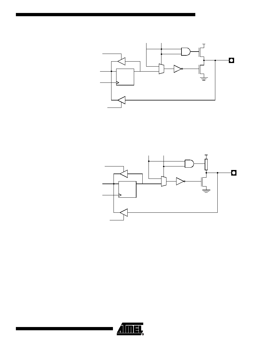
Figure 2. Port 0 Structure
Notes:
1. Port 0 is precluded from use as general-purpose I/O Ports when used as
address/data bus drivers.
2. Port 0 internal strong pull-ups assist the logic-one output for memory bus cycles only.
Except for these bus cycles, the pull-up FET is off, Port 0 outputs are open-drain.
Figure 3. Port 2 Structure
Notes:
1. Port 2 is precluded from use as general-purpose I/O Ports when as address/data bus
drivers.
2. Port 2 internal strong pull-ups FET (P1 in FiGURE) assist the logic-one output for
memory bus cycle.
When Port 0 and Port 2 are used for an external memory cycle, an internal control signal
switches the output-driver input from the latch output to the internal address/data line.
Read-Modify-Write
Instructions
Some instructions read the latch data rather than the pin data. The latch based instruc-
tions read the data, modify the data and then rewrite the latch. These are called "Read-
Modify-Write" instructions. Below is a complete list of these special instructions (see
Table ). When the destination operand is a Port or a Port bit, these instructions read the
latch rather than the pin:
D
Q
P0.X
LATCH
INTERNAL
WRITE
TO
LATCH
READ
PIN
READ
LATCH
0
1
P0.x (1)
ADDRESS LOW/
DATA
CONTROL
VDD
BUS
(2)
D
Q
P2.X
LATCH
INTERNAL
WRITE
TO
LATCH
READ
PIN
READ
LATCH
0
1
P2.x (1)
ADDRESS HIGH/ CONTROL
BUS
VDD
INTERNAL
PULL-UP (2)
相关PDF资料 |
PDF描述 |
|---|---|
| VE-B5R-IW-F4 | CONVERTER MOD DC/DC 7.5V 100W |
| VE-B5R-IW-F3 | CONVERTER MOD DC/DC 7.5V 100W |
| VE-B5R-IW-F2 | CONVERTER MOD DC/DC 7.5V 100W |
| VE-B5P-IX-F3 | CONVERTER MOD DC/DC 13.8V 75W |
| VE-B5P-IX-F1 | CONVERTER MOD DC/DC 13.8V 75W |
相关代理商/技术参数 |
参数描述 |
|---|---|
| AT89C51CC01UA-RLTUM | 功能描述:8位微控制器 -MCU CAN Bootloader UART RoHS:否 制造商:Silicon Labs 核心:8051 处理器系列:C8051F39x 数据总线宽度:8 bit 最大时钟频率:50 MHz 程序存储器大小:16 KB 数据 RAM 大小:1 KB 片上 ADC:Yes 工作电源电压:1.8 V to 3.6 V 工作温度范围:- 40 C to + 105 C 封装 / 箱体:QFN-20 安装风格:SMD/SMT |
| AT89C51CC01UA-SLSUM | 功能描述:8位微控制器 -MCU CAN-STICK Bootloader UART IND RoHS:否 制造商:Silicon Labs 核心:8051 处理器系列:C8051F39x 数据总线宽度:8 bit 最大时钟频率:50 MHz 程序存储器大小:16 KB 数据 RAM 大小:1 KB 片上 ADC:Yes 工作电源电压:1.8 V to 3.6 V 工作温度范围:- 40 C to + 105 C 封装 / 箱体:QFN-20 安装风格:SMD/SMT |
| AT89C51CC01UU-RLTUM | 功能描述:8位微控制器 -MCU Microcontroller RoHS:否 制造商:Silicon Labs 核心:8051 处理器系列:C8051F39x 数据总线宽度:8 bit 最大时钟频率:50 MHz 程序存储器大小:16 KB 数据 RAM 大小:1 KB 片上 ADC:Yes 工作电源电压:1.8 V to 3.6 V 工作温度范围:- 40 C to + 105 C 封装 / 箱体:QFN-20 安装风格:SMD/SMT |
| AT89C51CC01UU-SLSUM | 功能描述:8位微控制器 -MCU Microcontroller RoHS:否 制造商:Silicon Labs 核心:8051 处理器系列:C8051F39x 数据总线宽度:8 bit 最大时钟频率:50 MHz 程序存储器大小:16 KB 数据 RAM 大小:1 KB 片上 ADC:Yes 工作电源电压:1.8 V to 3.6 V 工作温度范围:- 40 C to + 105 C 封装 / 箱体:QFN-20 安装风格:SMD/SMT |
| AT89C51CC02 | 制造商:ATMEL 制造商全称:ATMEL Corporation 功能描述:Enhanced 8-bit Microcontroller with CAN Controller and Flash |
发布紧急采购,3分钟左右您将得到回复。