- 您现在的位置:买卖IC网 > PDF目录11806 > AT89C51CC01UA-RLRUM (Atmel)IC 8051 MCU 32K FLASH 44-VQFP PDF资料下载
参数资料
| 型号: | AT89C51CC01UA-RLRUM |
| 厂商: | Atmel |
| 文件页数: | 85/123页 |
| 文件大小: | 0K |
| 描述: | IC 8051 MCU 32K FLASH 44-VQFP |
| 产品培训模块: | MCU Product Line Introduction |
| 标准包装: | 1,500 |
| 系列: | AT89C CAN |
| 核心处理器: | 8051 |
| 芯体尺寸: | 8-位 |
| 速度: | 40MHz |
| 连通性: | CAN,UART/USART |
| 外围设备: | POR,PWM,WDT |
| 输入/输出数: | 34 |
| 程序存储器容量: | 32KB(32K x 8) |
| 程序存储器类型: | 闪存 |
| EEPROM 大小: | 2K x 8 |
| RAM 容量: | 1.25K x 8 |
| 电压 - 电源 (Vcc/Vdd): | 3 V ~ 5.5 V |
| 数据转换器: | A/D 8x10b |
| 振荡器型: | 外部 |
| 工作温度: | -40°C ~ 85°C |
| 封装/外壳: | 44-LQFP |
| 包装: | 标准包装 |
| 配用: | AT89OCD-01-ND - USB EMULATOR FOR AT8XC51 MCU |
| 其它名称: | AT89C51CC01UA-RLRUMDKR |
第1页第2页第3页第4页第5页第6页第7页第8页第9页第10页第11页第12页第13页第14页第15页第16页第17页第18页第19页第20页第21页第22页第23页第24页第25页第26页第27页第28页第29页第30页第31页第32页第33页第34页第35页第36页第37页第38页第39页第40页第41页第42页第43页第44页第45页第46页第47页第48页第49页第50页第51页第52页第53页第54页第55页第56页第57页第58页第59页第60页第61页第62页第63页第64页第65页第66页第67页第68页第69页第70页第71页第72页第73页第74页第75页第76页第77页第78页第79页第80页第81页第82页第83页第84页当前第85页第86页第87页第88页第89页第90页第91页第92页第93页第94页第95页第96页第97页第98页第99页第100页第101页第102页第103页第104页第105页第106页第107页第108页第109页第110页第111页第112页第113页第114页第115页第116页第117页第118页第119页第120页第121页第122页第123页
24
A/T89C51CC01
4129N–CAN–03/08
Internal Space
Lower 128 Bytes RAM
The lower 128 Bytes of RAM (see Figure 11) are accessible from address 00h to 7Fh
using direct or indirect addressing modes. The lowest 32 Bytes are grouped into 4
banks of 8 registers (R0 to R7). Two bits RS0 and RS1 in PSW register (see Figure 18)
select which bank is in use according to Table 16. This allows more efficient use of code
space, since register instructions are shorter than instructions that use direct address-
ing, and can be used for context switching in interrupt service routines.
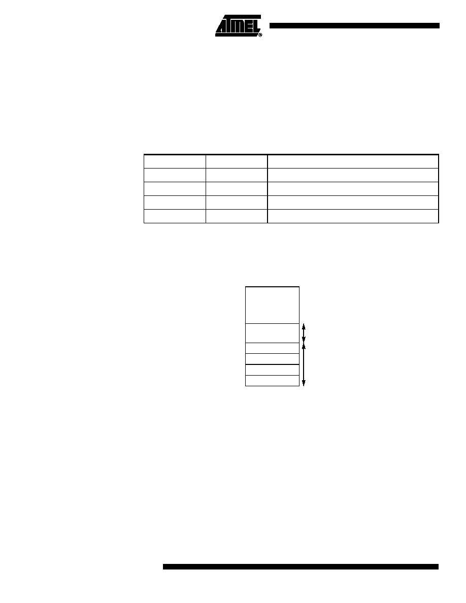
Table 16. Register Bank Selection
The next 16 Bytes above the register banks form a block of bit-addressable memory
space. The C51 instruction set includes a wide selection of single-bit instructions, and
the 128 bits in this area can be directly addressed by these instructions. The bit
addresses in this area are 00h to 7Fh.
Figure 12. Lower 128 Bytes Internal RAM Organization
Upper 128 Bytes RAM
The upper 128 Bytes of RAM are accessible from address 80h to FFh using only indirect
addressing mode.
Expanded RAM
The on-chip 1024 Bytes of expanded RAM (XRAM) are accessible from address 0000h
to 03FFh using indirect addressing mode through MOVX instructions. In this address
range, the bit EXTRAM in AUXR register is used to select the XRAM (default) or the
XRAM. As shown in Figure 11 when EXTRAM = 0, the XRAM is selected and when
EXTRAM = 1, the XRAM is selected.
The size of XRAM can be configured by XRS1-0 bit in AUXR register (default size is
1024 Bytes).
Note:
Lower 128 Bytes RAM, Upper 128 Bytes RAM, and expanded RAM are made of volatile
memory cells. This means that the RAM content is indeterminate after power-up and
must then be initialized properly.
RS1
RS0
Description
0
Register bank 0 from 00h to 07h
0
1
Register bank 0 from 08h to 0Fh
1
0
Register bank 0 from 10h to 17h
1
Register bank 0 from 18h to 1Fh
Bit-Addressable Space
4 Banks of
8 Registers
R0-R7
30h
7Fh
(Bit Addresses 0-7Fh)
20h
2Fh
18h
1Fh
10h
17h
08h
0Fh
00h
07h
相关PDF资料 |
PDF描述 |
|---|---|
| VE-B5R-IW-F4 | CONVERTER MOD DC/DC 7.5V 100W |
| VE-B5R-IW-F3 | CONVERTER MOD DC/DC 7.5V 100W |
| VE-B5R-IW-F2 | CONVERTER MOD DC/DC 7.5V 100W |
| VE-B5P-IX-F3 | CONVERTER MOD DC/DC 13.8V 75W |
| VE-B5P-IX-F1 | CONVERTER MOD DC/DC 13.8V 75W |
相关代理商/技术参数 |
参数描述 |
|---|---|
| AT89C51CC01UA-RLTUM | 功能描述:8位微控制器 -MCU CAN Bootloader UART RoHS:否 制造商:Silicon Labs 核心:8051 处理器系列:C8051F39x 数据总线宽度:8 bit 最大时钟频率:50 MHz 程序存储器大小:16 KB 数据 RAM 大小:1 KB 片上 ADC:Yes 工作电源电压:1.8 V to 3.6 V 工作温度范围:- 40 C to + 105 C 封装 / 箱体:QFN-20 安装风格:SMD/SMT |
| AT89C51CC01UA-SLSUM | 功能描述:8位微控制器 -MCU CAN-STICK Bootloader UART IND RoHS:否 制造商:Silicon Labs 核心:8051 处理器系列:C8051F39x 数据总线宽度:8 bit 最大时钟频率:50 MHz 程序存储器大小:16 KB 数据 RAM 大小:1 KB 片上 ADC:Yes 工作电源电压:1.8 V to 3.6 V 工作温度范围:- 40 C to + 105 C 封装 / 箱体:QFN-20 安装风格:SMD/SMT |
| AT89C51CC01UU-RLTUM | 功能描述:8位微控制器 -MCU Microcontroller RoHS:否 制造商:Silicon Labs 核心:8051 处理器系列:C8051F39x 数据总线宽度:8 bit 最大时钟频率:50 MHz 程序存储器大小:16 KB 数据 RAM 大小:1 KB 片上 ADC:Yes 工作电源电压:1.8 V to 3.6 V 工作温度范围:- 40 C to + 105 C 封装 / 箱体:QFN-20 安装风格:SMD/SMT |
| AT89C51CC01UU-SLSUM | 功能描述:8位微控制器 -MCU Microcontroller RoHS:否 制造商:Silicon Labs 核心:8051 处理器系列:C8051F39x 数据总线宽度:8 bit 最大时钟频率:50 MHz 程序存储器大小:16 KB 数据 RAM 大小:1 KB 片上 ADC:Yes 工作电源电压:1.8 V to 3.6 V 工作温度范围:- 40 C to + 105 C 封装 / 箱体:QFN-20 安装风格:SMD/SMT |
| AT89C51CC02 | 制造商:ATMEL 制造商全称:ATMEL Corporation 功能描述:Enhanced 8-bit Microcontroller with CAN Controller and Flash |
发布紧急采购,3分钟左右您将得到回复。