参数资料
| 型号: | AT89LP428-20AU |
| 厂商: | Atmel |
| 文件页数: | 109/149页 |
| 文件大小: | 0K |
| 描述: | MCU 8051 4K FLASH SPI 32TQFP |
| 产品培训模块: | MCU Product Line Introduction |
| 标准包装: | 250 |
| 系列: | 89LP |
| 核心处理器: | 8051 |
| 芯体尺寸: | 8-位 |
| 速度: | 20MHz |
| 连通性: | SPI,UART/USART |
| 外围设备: | 欠压检测/复位,POR,PWM,WDT |
| 输入/输出数: | 30 |
| 程序存储器容量: | 4KB(4K x 8) |
| 程序存储器类型: | 闪存 |
| EEPROM 大小: | 512 x 8 |
| RAM 容量: | 768 x 8 |
| 电压 - 电源 (Vcc/Vdd): | 2.4 V ~ 5.5 V |
| 振荡器型: | 内部 |
| 工作温度: | -40°C ~ 85°C |
| 封装/外壳: | 32-TQFP |
| 包装: | 托盘 |
第1页第2页第3页第4页第5页第6页第7页第8页第9页第10页第11页第12页第13页第14页第15页第16页第17页第18页第19页第20页第21页第22页第23页第24页第25页第26页第27页第28页第29页第30页第31页第32页第33页第34页第35页第36页第37页第38页第39页第40页第41页第42页第43页第44页第45页第46页第47页第48页第49页第50页第51页第52页第53页第54页第55页第56页第57页第58页第59页第60页第61页第62页第63页第64页第65页第66页第67页第68页第69页第70页第71页第72页第73页第74页第75页第76页第77页第78页第79页第80页第81页第82页第83页第84页第85页第86页第87页第88页第89页第90页第91页第92页第93页第94页第95页第96页第97页第98页第99页第100页第101页第102页第103页第104页第105页第106页第107页第108页当前第109页第110页第111页第112页第113页第114页第115页第116页第117页第118页第119页第120页第121页第122页第123页第124页第125页第126页第127页第128页第129页第130页第131页第132页第133页第134页第135页第136页第137页第138页第139页第140页第141页第142页第143页第144页第145页第146页第147页第148页第149页
62
3654A–MICRO–8/09
AT89LP428/828
Timer 2 must be running (TR2 = 1) in order to perform captures or compares with the CCA.
However, when TR2 = 0 the external capture events will still set their associated flags and may
be used as additional external interrupts.
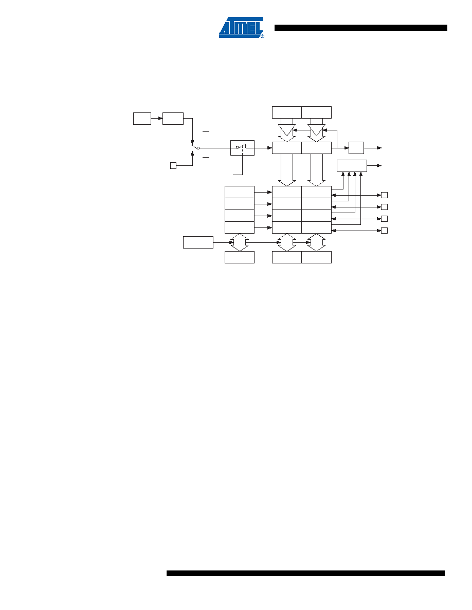
Figure 13-1. Compare/Capture Array Block Diagram
13.1
CCA Registers
The Compare/Capture Array has five Special Function Registers: T2CCA, T2CCC, T2CCL,
T2CCH and T2CCF. The T2CCF register contains the interrupt flags for each CCA channel. The
CCA interrupt is a logic OR of the bits in T2CCF. The flags are set by hardware when a com-
pare/capture event occurs on the relevant channel and must be cleared by software. The
T2CCF bits will only generate an interrupt when the ECC bit (IE2.1) is set and the CIENx bit in
the associated channel’s CCCx register is set.
The T2CCC, T2CCL and T2CCH register locations are not true SFRs. These locations represent
access points to the contents of the array. Writes/reads to/from the T2CCC, T2CCL and T2CCH
locations will access the control, data low and data high bytes of the CCA channel currently
selected by the index in T2CCA. Channels currently not indexed by T2CCA are not accessible.
When writing to T2CCH, the value is stored in a shadow register. When T2CCL is written, the
16-bit value formed by the contents of T2CCL and the T2CCH shadow is written into the array.
Therefore, T2CCH must be written prior to writing T2CCL. All four channels use the same
T2CCH shadow register. If the value of T2CCH remains constant for multiple writes, there is no
need to update T2CCH between T2CCL writes. Every write to T2CCL will use the last value of
T2CCH for the upper data byte. It is not possible to write to the data register of a channel config-
ured for capture mode.
The configuration bits for each channel are stored in the CCCx registers accessible through
T2CCC. See Table 13-4 on page 64 for a description of the CCCx register.
OSC
(P1.0) T2
TR2
TL2
Timer 2 Interrupt
C/T2 = 0
C/T2 =1
TH2
TF2
RCAP2L
RCAP2H
÷TPS
CCAL
CCAH
CCCA
CCBL
CCBH
CCCB
CCCL
CCCH
CCCC
CCDL
CCDH
CCCD
T2CCF
CCA Interrupt
CCA (P2.0)
CCB (P2.1)
CCC (P2.2)
CCD (P2.3)
T2CCC
T2CCL
T2CCH
T2CCA
相关PDF资料 |
PDF描述 |
|---|---|
| AT89LP52-20MU | IC MCU 8051 8K FLASH SPI 44VQFN |
| AT89LP6440-20JU | MCU 8051 64K FLASH ISP 44PLCC |
| AT89LP828-JU | IC MCU 8051 8KB FLASH 32PLCC |
| AT89LS51-16AU | IC MCU 4K FLASH 16MHZ 44-TQFP |
| AT89LS52-16PU | IC MCU 8K FLASH 16MHZ 40-DIP |
相关代理商/技术参数 |
参数描述 |
|---|---|
| AT89LP428-20JU | 功能描述:8位微控制器 -MCU SingleCycle 8051 4K ISP Flash 2.4V RoHS:否 制造商:Silicon Labs 核心:8051 处理器系列:C8051F39x 数据总线宽度:8 bit 最大时钟频率:50 MHz 程序存储器大小:16 KB 数据 RAM 大小:1 KB 片上 ADC:Yes 工作电源电压:1.8 V to 3.6 V 工作温度范围:- 40 C to + 105 C 封装 / 箱体:QFN-20 安装风格:SMD/SMT |
| AT89LP428-20MH | 功能描述:8位微控制器 -MCU SingleCycle 8051 4K ISP Flash 2.4V RoHS:否 制造商:Silicon Labs 核心:8051 处理器系列:C8051F39x 数据总线宽度:8 bit 最大时钟频率:50 MHz 程序存储器大小:16 KB 数据 RAM 大小:1 KB 片上 ADC:Yes 工作电源电压:1.8 V to 3.6 V 工作温度范围:- 40 C to + 105 C 封装 / 箱体:QFN-20 安装风格:SMD/SMT |
| AT89LP428-20PU | 功能描述:8位微控制器 -MCU SingleCycle 8051 4K ISP Flash 2.4V RoHS:否 制造商:Silicon Labs 核心:8051 处理器系列:C8051F39x 数据总线宽度:8 bit 最大时钟频率:50 MHz 程序存储器大小:16 KB 数据 RAM 大小:1 KB 片上 ADC:Yes 工作电源电压:1.8 V to 3.6 V 工作温度范围:- 40 C to + 105 C 封装 / 箱体:QFN-20 安装风格:SMD/SMT |
| AT89LP51-20AU | 功能描述:8位微控制器 -MCU Single Cycle 8051 4K ISP FL RoHS:否 制造商:Silicon Labs 核心:8051 处理器系列:C8051F39x 数据总线宽度:8 bit 最大时钟频率:50 MHz 程序存储器大小:16 KB 数据 RAM 大小:1 KB 片上 ADC:Yes 工作电源电压:1.8 V to 3.6 V 工作温度范围:- 40 C to + 105 C 封装 / 箱体:QFN-20 安装风格:SMD/SMT |
| AT89LP51-20JU | 功能描述:8位微控制器 -MCU Single Cycle 8051 4K ISP FL RoHS:否 制造商:Silicon Labs 核心:8051 处理器系列:C8051F39x 数据总线宽度:8 bit 最大时钟频率:50 MHz 程序存储器大小:16 KB 数据 RAM 大小:1 KB 片上 ADC:Yes 工作电源电压:1.8 V to 3.6 V 工作温度范围:- 40 C to + 105 C 封装 / 箱体:QFN-20 安装风格:SMD/SMT |
发布紧急采购,3分钟左右您将得到回复。