参数资料
| 型号: | AT89LP428-20AU |
| 厂商: | Atmel |
| 文件页数: | 18/149页 |
| 文件大小: | 0K |
| 描述: | MCU 8051 4K FLASH SPI 32TQFP |
| 产品培训模块: | MCU Product Line Introduction |
| 标准包装: | 250 |
| 系列: | 89LP |
| 核心处理器: | 8051 |
| 芯体尺寸: | 8-位 |
| 速度: | 20MHz |
| 连通性: | SPI,UART/USART |
| 外围设备: | 欠压检测/复位,POR,PWM,WDT |
| 输入/输出数: | 30 |
| 程序存储器容量: | 4KB(4K x 8) |
| 程序存储器类型: | 闪存 |
| EEPROM 大小: | 512 x 8 |
| RAM 容量: | 768 x 8 |
| 电压 - 电源 (Vcc/Vdd): | 2.4 V ~ 5.5 V |
| 振荡器型: | 内部 |
| 工作温度: | -40°C ~ 85°C |
| 封装/外壳: | 32-TQFP |
| 包装: | 托盘 |
第1页第2页第3页第4页第5页第6页第7页第8页第9页第10页第11页第12页第13页第14页第15页第16页第17页当前第18页第19页第20页第21页第22页第23页第24页第25页第26页第27页第28页第29页第30页第31页第32页第33页第34页第35页第36页第37页第38页第39页第40页第41页第42页第43页第44页第45页第46页第47页第48页第49页第50页第51页第52页第53页第54页第55页第56页第57页第58页第59页第60页第61页第62页第63页第64页第65页第66页第67页第68页第69页第70页第71页第72页第73页第74页第75页第76页第77页第78页第79页第80页第81页第82页第83页第84页第85页第86页第87页第88页第89页第90页第91页第92页第93页第94页第95页第96页第97页第98页第99页第100页第101页第102页第103页第104页第105页第106页第107页第108页第109页第110页第111页第112页第113页第114页第115页第116页第117页第118页第119页第120页第121页第122页第123页第124页第125页第126页第127页第128页第129页第130页第131页第132页第133页第134页第135页第136页第137页第138页第139页第140页第141页第142页第143页第144页第145页第146页第147页第148页第149页
114
3654A–MICRO–8/09
AT89LP428/828
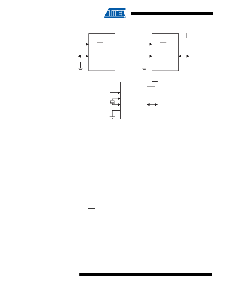
Figure 22-1. AT89LP428/828 On-chip Debug Connections
22.2
Software Breakpoints
The AT89LP428/828 microcontroller includes a BREAK instruction for implementing program
memory breakpoints in software. A software breakpoint can be inserted manually by placing the
BREAK instruction in the program code. Some emulator systems may allow for automatic inser-
tion/deletion of software breakpoints. The Flash memory must be re-programmed each time a
software breakpoint is changed. Frequent insertions/deletions of software breakpoints will
reduce the endurance of the nonvolatile memory. Devices used for debugging purposes should
not be shipped to end customers. The BREAK instruction is treated as a two-cycle NOP when
OCD is disabled.
22.3
Limitations of On-chip Debug
The AT89LP428/828 is a fully-featured microcontroller that multiplexes several functions on its
limited I/O pins. Some device functionality must be sacrificed to provide resources for On-chip
Debugging. The On-chip Debug System has the following limitations:
The Debug Clock pin (DCL) is physically located on that same pin as Port Pin P3.6 and the
External Reset (RST). Therefore, neither P3.6 nor an external reset source may be emulated
when OCD is enabled.
When using the Internal RC Oscillator during debug, DDA is located on the XTAL1/P4.0 pin.
The P4.0 I/O function cannot be emulated in this mode.
When using the External Clock during debug, DDA is located on the XTAL2/P4.1 pin and the
system clock drives XTAL1/P4.0. The P4.1 I/O and CLKOUT functions cannot be emulated in
this mode.
When using the Crystal Oscillator during debug, DDA is located on the P3.7 pin and the
crystal connects to XTAL1/P4.0 and XTAL2/P4.1. The P3.6 I/O function cannot be emulated
in this mode.
CLK = Internal RC
VCC
XTAL1
P3.6/RST
GND
DCL
DDA
CLK = External Clock
VCC
XTAL2
P3.6/RST
GND
DCL
DDA
XTAL1
CLK
CLK = Crystal Oscillator
VCC
P3.7
P3.6/RST
GND
DCL
DDA
XTAL1
XTAL2
AB
C
相关PDF资料 |
PDF描述 |
|---|---|
| AT89LP52-20MU | IC MCU 8051 8K FLASH SPI 44VQFN |
| AT89LP6440-20JU | MCU 8051 64K FLASH ISP 44PLCC |
| AT89LP828-JU | IC MCU 8051 8KB FLASH 32PLCC |
| AT89LS51-16AU | IC MCU 4K FLASH 16MHZ 44-TQFP |
| AT89LS52-16PU | IC MCU 8K FLASH 16MHZ 40-DIP |
相关代理商/技术参数 |
参数描述 |
|---|---|
| AT89LP428-20JU | 功能描述:8位微控制器 -MCU SingleCycle 8051 4K ISP Flash 2.4V RoHS:否 制造商:Silicon Labs 核心:8051 处理器系列:C8051F39x 数据总线宽度:8 bit 最大时钟频率:50 MHz 程序存储器大小:16 KB 数据 RAM 大小:1 KB 片上 ADC:Yes 工作电源电压:1.8 V to 3.6 V 工作温度范围:- 40 C to + 105 C 封装 / 箱体:QFN-20 安装风格:SMD/SMT |
| AT89LP428-20MH | 功能描述:8位微控制器 -MCU SingleCycle 8051 4K ISP Flash 2.4V RoHS:否 制造商:Silicon Labs 核心:8051 处理器系列:C8051F39x 数据总线宽度:8 bit 最大时钟频率:50 MHz 程序存储器大小:16 KB 数据 RAM 大小:1 KB 片上 ADC:Yes 工作电源电压:1.8 V to 3.6 V 工作温度范围:- 40 C to + 105 C 封装 / 箱体:QFN-20 安装风格:SMD/SMT |
| AT89LP428-20PU | 功能描述:8位微控制器 -MCU SingleCycle 8051 4K ISP Flash 2.4V RoHS:否 制造商:Silicon Labs 核心:8051 处理器系列:C8051F39x 数据总线宽度:8 bit 最大时钟频率:50 MHz 程序存储器大小:16 KB 数据 RAM 大小:1 KB 片上 ADC:Yes 工作电源电压:1.8 V to 3.6 V 工作温度范围:- 40 C to + 105 C 封装 / 箱体:QFN-20 安装风格:SMD/SMT |
| AT89LP51-20AU | 功能描述:8位微控制器 -MCU Single Cycle 8051 4K ISP FL RoHS:否 制造商:Silicon Labs 核心:8051 处理器系列:C8051F39x 数据总线宽度:8 bit 最大时钟频率:50 MHz 程序存储器大小:16 KB 数据 RAM 大小:1 KB 片上 ADC:Yes 工作电源电压:1.8 V to 3.6 V 工作温度范围:- 40 C to + 105 C 封装 / 箱体:QFN-20 安装风格:SMD/SMT |
| AT89LP51-20JU | 功能描述:8位微控制器 -MCU Single Cycle 8051 4K ISP FL RoHS:否 制造商:Silicon Labs 核心:8051 处理器系列:C8051F39x 数据总线宽度:8 bit 最大时钟频率:50 MHz 程序存储器大小:16 KB 数据 RAM 大小:1 KB 片上 ADC:Yes 工作电源电压:1.8 V to 3.6 V 工作温度范围:- 40 C to + 105 C 封装 / 箱体:QFN-20 安装风格:SMD/SMT |
发布紧急采购,3分钟左右您将得到回复。