参数资料
| 型号: | AT89LP428-20AU |
| 厂商: | Atmel |
| 文件页数: | 113/149页 |
| 文件大小: | 0K |
| 描述: | MCU 8051 4K FLASH SPI 32TQFP |
| 产品培训模块: | MCU Product Line Introduction |
| 标准包装: | 250 |
| 系列: | 89LP |
| 核心处理器: | 8051 |
| 芯体尺寸: | 8-位 |
| 速度: | 20MHz |
| 连通性: | SPI,UART/USART |
| 外围设备: | 欠压检测/复位,POR,PWM,WDT |
| 输入/输出数: | 30 |
| 程序存储器容量: | 4KB(4K x 8) |
| 程序存储器类型: | 闪存 |
| EEPROM 大小: | 512 x 8 |
| RAM 容量: | 768 x 8 |
| 电压 - 电源 (Vcc/Vdd): | 2.4 V ~ 5.5 V |
| 振荡器型: | 内部 |
| 工作温度: | -40°C ~ 85°C |
| 封装/外壳: | 32-TQFP |
| 包装: | 托盘 |
第1页第2页第3页第4页第5页第6页第7页第8页第9页第10页第11页第12页第13页第14页第15页第16页第17页第18页第19页第20页第21页第22页第23页第24页第25页第26页第27页第28页第29页第30页第31页第32页第33页第34页第35页第36页第37页第38页第39页第40页第41页第42页第43页第44页第45页第46页第47页第48页第49页第50页第51页第52页第53页第54页第55页第56页第57页第58页第59页第60页第61页第62页第63页第64页第65页第66页第67页第68页第69页第70页第71页第72页第73页第74页第75页第76页第77页第78页第79页第80页第81页第82页第83页第84页第85页第86页第87页第88页第89页第90页第91页第92页第93页第94页第95页第96页第97页第98页第99页第100页第101页第102页第103页第104页第105页第106页第107页第108页第109页第110页第111页第112页当前第113页第114页第115页第116页第117页第118页第119页第120页第121页第122页第123页第124页第125页第126页第127页第128页第129页第130页第131页第132页第133页第134页第135页第136页第137页第138页第139页第140页第141页第142页第143页第144页第145页第146页第147页第148页第149页
66
3654A–MICRO–8/09
AT89LP428/828
Each CCA channel has an associated external capture input pin: CCA (P2.0), CCB (P2.1), CCC
(P2.2) and CCD (P2.3). External capture events are always edge-triggered and can be selected
to occur at a negative edge, positive edge, or both (toggle). Capture inputs are sampled every
clock cycle and a new value must be held for at least 2 clock cycles to be correctly sampled by
the device. The maximum achievable capture rate will be determined by how fast the software
can retrieve the captured data. There is no protection against capture events overrunning the
data register.
Capture events may also be triggered internally by the overflows of Timer 0 or Timer 1, or by an
event from the dual analog comparators. Any comparator event which can generate a compara-
tor interrupt may also be used as a capture event. However, Timer 2 should not be selected as
the comparator clock source when using the comparator as the capture trigger.
13.2.1
Timer 2 Operation for Capture Mode
Capture channels are intended to work with Timer 2 in capture mode CP/RL2 =1. Captures can
still occur when Timer 2 operates in other modes; however, the full 16-bit count range may not
be available. The TF2 flag can be used to determine if the timer overflowed before the capture
occurred. If the timer is operating in dual-slope mode (CP/RL2 =0, T2CM
1-0 =1xB), the count
direction (Up = 0 and Down = 1) at the time of the event will be captured into the channel’s
CDIRx bit in CCCx. CTCx must be cleared to 0 for all channels if Timer 2 is operating in Baud
Rate mode or errors may occur in the serial communication.
13.3
Output Compare Mode
The Compare/Capture Array provides a variety of compare modes suitable for event timing or
waveform generation. The CCA channels are configured for compare mode by setting the CCMx
bit in the associated CCCx register to 1. A compare event occurs when the 16-bit contents of a
channel’s data register match the contents of Timer 2 (TH2 and TL2). The compare event also
sets the channel’s interrupt flag CCFx in T2CCF and may optionally clear Timer 2 to 0000H if the
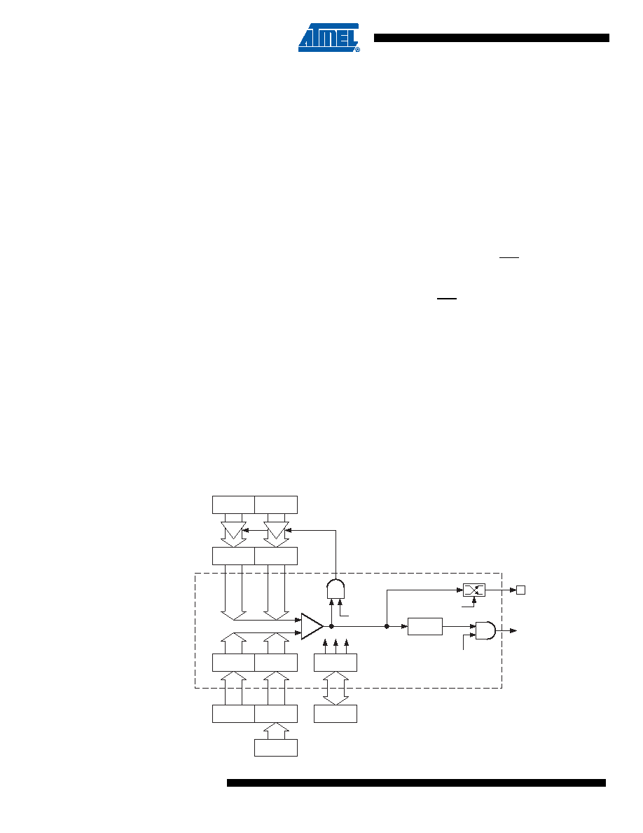
CTCx bit in CCCx is set. A diagram of a CCA channel in compare mode is shown in Figure 13-3.
Figure 13-3. CCA Compare Mode Diagram
TL2
TH2
CCxL
CCxH
CCCx
Interrupt
CCx (P2.x)
T2CCC
T2CCL
Shadow
00H
CTCx
CCFx
CIENx
CxM2-0
=
T2CCH
相关PDF资料 |
PDF描述 |
|---|---|
| AT89LP52-20MU | IC MCU 8051 8K FLASH SPI 44VQFN |
| AT89LP6440-20JU | MCU 8051 64K FLASH ISP 44PLCC |
| AT89LP828-JU | IC MCU 8051 8KB FLASH 32PLCC |
| AT89LS51-16AU | IC MCU 4K FLASH 16MHZ 44-TQFP |
| AT89LS52-16PU | IC MCU 8K FLASH 16MHZ 40-DIP |
相关代理商/技术参数 |
参数描述 |
|---|---|
| AT89LP428-20JU | 功能描述:8位微控制器 -MCU SingleCycle 8051 4K ISP Flash 2.4V RoHS:否 制造商:Silicon Labs 核心:8051 处理器系列:C8051F39x 数据总线宽度:8 bit 最大时钟频率:50 MHz 程序存储器大小:16 KB 数据 RAM 大小:1 KB 片上 ADC:Yes 工作电源电压:1.8 V to 3.6 V 工作温度范围:- 40 C to + 105 C 封装 / 箱体:QFN-20 安装风格:SMD/SMT |
| AT89LP428-20MH | 功能描述:8位微控制器 -MCU SingleCycle 8051 4K ISP Flash 2.4V RoHS:否 制造商:Silicon Labs 核心:8051 处理器系列:C8051F39x 数据总线宽度:8 bit 最大时钟频率:50 MHz 程序存储器大小:16 KB 数据 RAM 大小:1 KB 片上 ADC:Yes 工作电源电压:1.8 V to 3.6 V 工作温度范围:- 40 C to + 105 C 封装 / 箱体:QFN-20 安装风格:SMD/SMT |
| AT89LP428-20PU | 功能描述:8位微控制器 -MCU SingleCycle 8051 4K ISP Flash 2.4V RoHS:否 制造商:Silicon Labs 核心:8051 处理器系列:C8051F39x 数据总线宽度:8 bit 最大时钟频率:50 MHz 程序存储器大小:16 KB 数据 RAM 大小:1 KB 片上 ADC:Yes 工作电源电压:1.8 V to 3.6 V 工作温度范围:- 40 C to + 105 C 封装 / 箱体:QFN-20 安装风格:SMD/SMT |
| AT89LP51-20AU | 功能描述:8位微控制器 -MCU Single Cycle 8051 4K ISP FL RoHS:否 制造商:Silicon Labs 核心:8051 处理器系列:C8051F39x 数据总线宽度:8 bit 最大时钟频率:50 MHz 程序存储器大小:16 KB 数据 RAM 大小:1 KB 片上 ADC:Yes 工作电源电压:1.8 V to 3.6 V 工作温度范围:- 40 C to + 105 C 封装 / 箱体:QFN-20 安装风格:SMD/SMT |
| AT89LP51-20JU | 功能描述:8位微控制器 -MCU Single Cycle 8051 4K ISP FL RoHS:否 制造商:Silicon Labs 核心:8051 处理器系列:C8051F39x 数据总线宽度:8 bit 最大时钟频率:50 MHz 程序存储器大小:16 KB 数据 RAM 大小:1 KB 片上 ADC:Yes 工作电源电压:1.8 V to 3.6 V 工作温度范围:- 40 C to + 105 C 封装 / 箱体:QFN-20 安装风格:SMD/SMT |
发布紧急采购,3分钟左右您将得到回复。