- 您现在的位置:买卖IC网 > PDF目录42901 > ATF-331M4-TR2 (AGILENT TECHNOLOGIES INC) X BAND, Si, N-CHANNEL, RF SMALL SIGNAL, HEMFET PDF资料下载
参数资料
| 型号: | ATF-331M4-TR2 |
| 厂商: | AGILENT TECHNOLOGIES INC |
| 元件分类: | 小信号晶体管 |
| 英文描述: | X BAND, Si, N-CHANNEL, RF SMALL SIGNAL, HEMFET |
| 封装: | MINIPAK-4 |
| 文件页数: | 9/16页 |
| 文件大小: | 212K |
| 代理商: | ATF-331M4-TR2 |
2
ATF-331M4 Absolute Maximum Ratings[1]
Absolute
Symbol
Parameter
Units
Maximum
V
DS
Drain-Source Voltage[2]
V
5.5
V
GS
Gate-Source Voltage[2]
V-5
V
GD
Gate Drain Voltage [2]
V-5
I
DS
Drain Current [2]
mA
Idiss
[3]
Pdiss
Total Power Dissipation [4]
mW
400
Pin max.
RF Input Power
dBm
20
T
CH
Channel Temperature[5]
°C
160
T
STG
Storage Temperature
°C
-65 to 160
θ
jc
Thermal Resistance [6]
°C/W
200
Notes:
1. Operation of this device above any one of
these parameters may cause permanent
damage.
2. Assumes DC quiescent conditions.
3. V
GS = 0 V
4. Source lead temperature is 25
°C. Derate
5 mW/
°C for T
L > 40°C.
5. Please refer to failure rates in reliability data
sheet to assess the reliability impact of
running devices above a channel temperature
of 140
°C.
6. Thermal resistance measured using 150
°C
Liquid Crystal Measurement method.
Product Consistency Distribution Charts [8, 9]
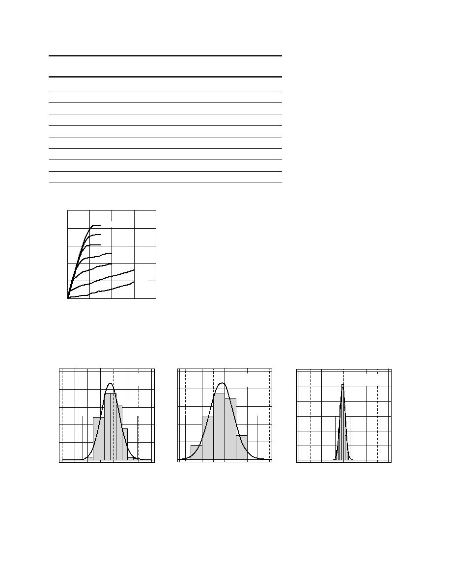
VDS (V)
Figure 1. Typical Pulsed I-V Curves[7].
(VGS = -0.2 V per step)
I DS
(mA)
02
4
6
8
500
400
300
200
100
0
-0.6 V
0 V
+0.6 V
NF (dBm)
Figure 2. NF @ 2 GHz, 4 V, 60 mA.
LSL = 28.5, Nominal = 0.6, USL = 0.8.
0.2
0.4
0.5
0.6
0.7
0.3
0.8
0.9
100
80
60
40
20
0
-3 Std
+3 Std
Cpk = 1.05
Stdev = 0.07
OIP3 (dBm)
Figure 3. OIP3 @ 2 GHz, 4 V, 60 mA.
LSL = 28.5, Nominal = 31.0, USL = 36.0
28
32
30
34
36
-3 Std
+3 Std
150
120
90
60
30
0
Cpk = 1.00
Stdev = 1.07
GAIN (dB)
Figure 4. Gain @ 2 GHz, 4 V, 60 mA.
LSL = 13.5, Nominal = 15.0, USL = 16.5
13
15
14
16
17
-3 Std
+3 Std
120
100
80
60
40
20
0
Cpk = 4.37
Stdev = 1.11
Notes:
8. Distribution data sample size is 349 samples from 4 different wafers. Future wafers allocated to this product may have nominal values anywhere within
the upper and lower spec limits.
9. Measurements made on production test board. This circuit represents a trade-off between an optimal noise match and a realizeable match based on
production test requirements. Circuit losses have been de-embedded from actual measurements.
Note:
7. Under large signal conditions, V
GS may swing
positive and the drain current may exceed
I
dss. These conditions are acceptable as long
as the Maximum Pdiss and Pin max ratings are
not exceeded.
相关PDF资料 |
PDF描述 |
|---|---|
| ATF-331M4-TR2G | X BAND, Si, N-CHANNEL, RF SMALL SIGNAL, HEMFET |
| ATF-331M4-TR1G | X BAND, Si, N-CHANNEL, RF SMALL SIGNAL, HEMFET |
| ATF-331M4-BLKG | X BAND, Si, N-CHANNEL, RF SMALL SIGNAL, HEMFET |
| ATF-34143-TR2G | X BAND, Si, N-CHANNEL, RF SMALL SIGNAL, HEMFET |
| ATF-34143-TR1G | X BAND, Si, N-CHANNEL, RF SMALL SIGNAL, HEMFET |
相关代理商/技术参数 |
参数描述 |
|---|---|
| ATF34143 | 制造商:HP 制造商全称:Agilent(Hewlett-Packard) 功能描述:Low Noise Pseudomorphic HEMT in a Surface Mount Plastic Package |
| ATF-34143 | 制造商:Avago Technologies 功能描述:MOSFET RF SOT-343 |
| ATF34143BLK | 制造商:未知厂家 制造商全称:未知厂家 功能描述:TRANSISTOR | JFET | N-CHANNEL | 5.5V V(BR)DSS | 90MA I(DSS) | SOT-343R |
| ATF-34143-BLK | 制造商:Agilent Technologies 功能描述:JFET Transistor, N-Channel, SOT-343R |
| ATF-34143-BLKG | 功能描述:射频GaAs晶体管 Transistor GaAs Low Noise RoHS:否 制造商:TriQuint Semiconductor 技术类型:pHEMT 频率:500 MHz to 3 GHz 增益:10 dB 噪声系数: 正向跨导 gFS(最大值/最小值):4 S 漏源电压 VDS: 闸/源击穿电压:- 8 V 漏极连续电流:3 A 最大工作温度:+ 150 C 功率耗散:10 W 安装风格: 封装 / 箱体: |
发布紧急采购,3分钟左右您将得到回复。