- 您现在的位置:买卖IC网 > PDF目录42903 > ATF-511P8-BLK C BAND, Si, N-CHANNEL, RF POWER, HEMFET PDF资料下载
参数资料
| 型号: | ATF-511P8-BLK |
| 元件分类: | 功率晶体管 |
| 英文描述: | C BAND, Si, N-CHANNEL, RF POWER, HEMFET |
| 封装: | 2 X 2 MM, 0.75 MM HEIGHT, LPCC-8 |
| 文件页数: | 9/16页 |
| 文件大小: | 447K |
| 代理商: | ATF-511P8-BLK |
2
ATF-511P8 Absolute Maximum Ratings[1]
Absolute
Symbol
Parameter
Units
Maximum
V
DS
Drain–Source Voltage[2]
V7
V
GS
Gate–Source Voltage[2]
V
-5 to 1
V
GD
Gate Drain Voltage[2]
V
-5 to 1
I
DS
Drain Current[2]
A1
I
GS
Gate Current
mA
46
P
diss
Total Power Dissipation[3]
W3
P
in max.
RF Input Power[4]
dBm
+30
T
CH
Channel Temperature
°C
150
T
STG
Storage Temperature
°C
-65 to 150
θ
ch_b
Thermal Resistance[5]
°C/W
33
Notes:
1. Operation of this device in excess of any one
of these parameters may cause permanent
damage.
2. Assumes DC quiescent conditions.
3. Board (package belly) temperatureT
B is 25°C.
Derate 30 mW/
°C for T
B > 50°C.
4. With 10 Ohm series resistor in gate supply
and 3:1 VSWR.
5. Channel-to-board thermal resistance
measured using 150
°C Liquid Crystal
Measurement method.
6. Device can safely handle +30dBm RF Input
Power provided I
GS limited to 46mA. IGS at
P1dB drive level is bias circuit dependent.
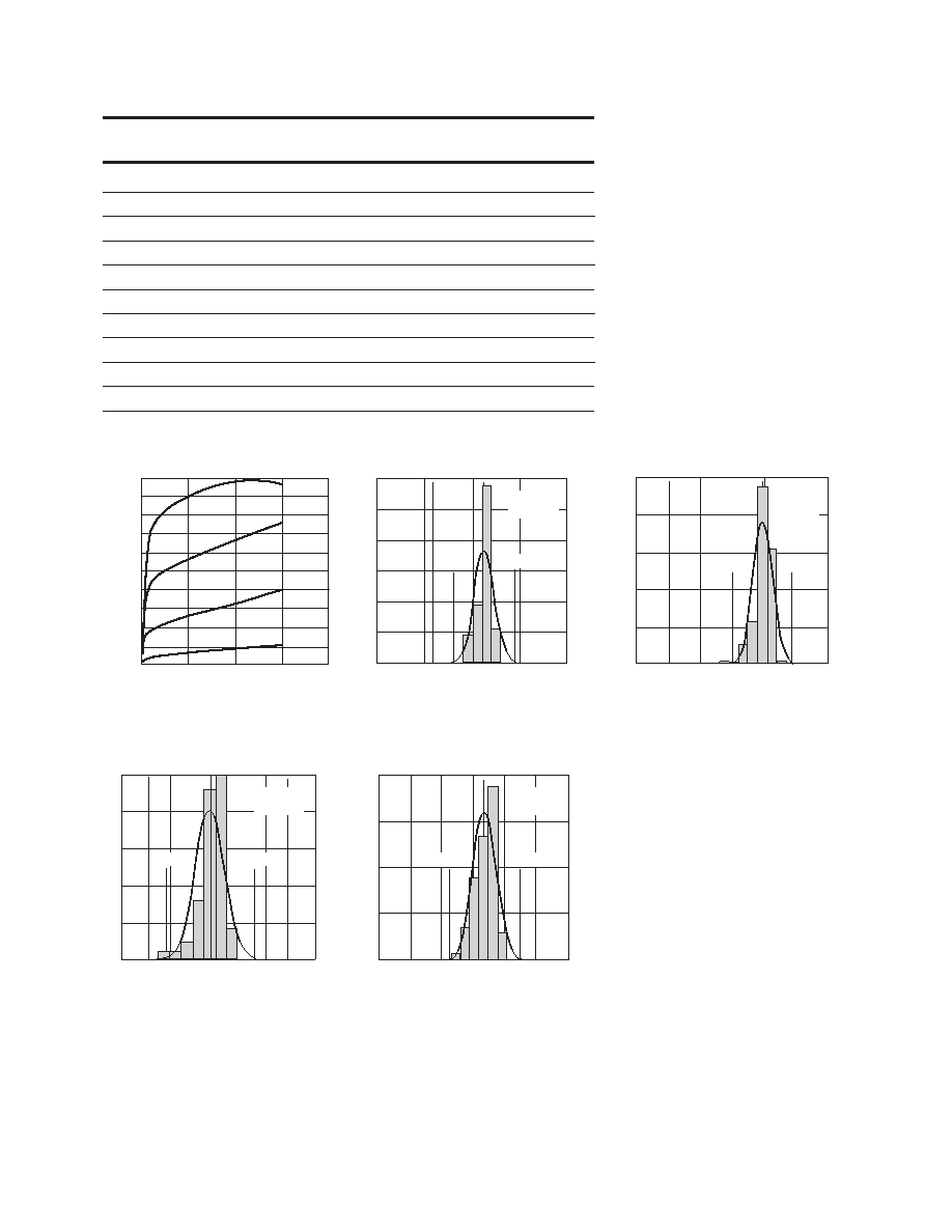
Product Consistency Distribution Charts at 2 GHz, 4.5V, 200 mA[6,7]
OIP3 (dBm)
Figure 2. OIP3
LSL = 38.5, Nominal = 41.7.
35
41
38
44
47
240
200
160
120
80
40
0
Cpk = 1.66
Stdev = 0.6
-3 Std
+3 Std
P1dB (dBm)
Figure 3. P1dB
LSL = 28.5, Nominal = 30.
28
30
29
31
200
160
120
80
40
0
Cpk = 3.24
Stdev = 0.15
-3 Std
+3 Std
GAIN (dB)
Figure 4. Gain
LSL = 13.5, Nominal = 14.8, USL = 16.5.
13
15
14
16
17
150
120
90
60
30
0
Cpk = 1.4
Stdev = 0.31
-3 Std
+3 Std
Notes:
6. Distribution data sample size is 400 samples taken from 4 different wafers and 3 different lots.
Future wafers allocated to this product may have nominal values anywhere between the upper and
lower limits.
7. Measurements are made on production test board, which represents a trade-off between optimal
OIP3, P1dB and VSWR. Circuit losses have been de-embedded from actual measurements.
Figure 1. Typical I-V Curves
(Vgs = 0.1 per step).
VDS (V)
1000
900
800
700
600
500
400
300
200
100
0
02
4
6
8
I DS
(mA)
0.8 V
0.7 V
0.5 V
0.6 V
PAE (%)
Figure 5. PAE
LSL = 52, Nominal = 68.9.
52
62
57
67
72
77
82
160
120
80
40
0
Cpk = 3.03
Stdev = 1.85
-3 Std
+3 Std
相关PDF资料 |
PDF描述 |
|---|---|
| ATF-52189-BLK | C BAND, Si, N-CHANNEL, RF SMALL SIGNAL, HEMFET |
| ATF-52189-TR1 | C BAND, Si, N-CHANNEL, RF SMALL SIGNAL, HEMFET |
| ATF-521P8-TR1 | C BAND, Si, N-CHANNEL, RF SMALL SIGNAL, HEMFET, MO-229 |
| ATF-521P8-TR2 | C BAND, Si, N-CHANNEL, RF SMALL SIGNAL, HEMFET, MO-229 |
| ATF-521P8-BLK | C BAND, Si, N-CHANNEL, RF SMALL SIGNAL, HEMFET, MO-229 |
相关代理商/技术参数 |
参数描述 |
|---|---|
| ATF-511P8-BLK | 制造商:Avago Technologies 功能描述:RF Bipolar Transistor |
| ATF-511P8-TR1 | 功能描述:射频GaAs晶体管 Transistor GaAs High Linearity RoHS:否 制造商:TriQuint Semiconductor 技术类型:pHEMT 频率:500 MHz to 3 GHz 增益:10 dB 噪声系数: 正向跨导 gFS(最大值/最小值):4 S 漏源电压 VDS: 闸/源击穿电压:- 8 V 漏极连续电流:3 A 最大工作温度:+ 150 C 功率耗散:10 W 安装风格: 封装 / 箱体: |
| ATF-511P8-TR2 | 功能描述:射频GaAs晶体管 Transistor GaAs High Linearity RoHS:否 制造商:TriQuint Semiconductor 技术类型:pHEMT 频率:500 MHz to 3 GHz 增益:10 dB 噪声系数: 正向跨导 gFS(最大值/最小值):4 S 漏源电压 VDS: 闸/源击穿电压:- 8 V 漏极连续电流:3 A 最大工作温度:+ 150 C 功率耗散:10 W 安装风格: 封装 / 箱体: |
| ATF-52189-BLK | 功能描述:射频GaAs晶体管 Transistor GaAs High Linearity RoHS:否 制造商:TriQuint Semiconductor 技术类型:pHEMT 频率:500 MHz to 3 GHz 增益:10 dB 噪声系数: 正向跨导 gFS(最大值/最小值):4 S 漏源电压 VDS: 闸/源击穿电压:- 8 V 漏极连续电流:3 A 最大工作温度:+ 150 C 功率耗散:10 W 安装风格: 封装 / 箱体: |
| ATF-52189-TR1 | 功能描述:射频GaAs晶体管 Transistor GaAs High Linearity RoHS:否 制造商:TriQuint Semiconductor 技术类型:pHEMT 频率:500 MHz to 3 GHz 增益:10 dB 噪声系数: 正向跨导 gFS(最大值/最小值):4 S 漏源电压 VDS: 闸/源击穿电压:- 8 V 漏极连续电流:3 A 最大工作温度:+ 150 C 功率耗散:10 W 安装风格: 封装 / 箱体: |
发布紧急采购,3分钟左右您将得到回复。