- 您现在的位置:买卖IC网 > PDF目录42904 > ATF-54143-BLK (AGILENT TECHNOLOGIES INC) C BAND, GaAs, N-CHANNEL, RF SMALL SIGNAL, HEMFET PDF资料下载
参数资料
| 型号: | ATF-54143-BLK |
| 厂商: | AGILENT TECHNOLOGIES INC |
| 元件分类: | 小信号晶体管 |
| 英文描述: | C BAND, GaAs, N-CHANNEL, RF SMALL SIGNAL, HEMFET |
| 封装: | PLASTIC, SC-70, 4 PIN |
| 文件页数: | 2/17页 |
| 文件大小: | 212K |
| 代理商: | ATF-54143-BLK |
10
ATF-54143 Applications
Information
Introduction
Agilent Technologies’s ATF-54143
is a low noise enhancement mode
PHEMT designed for use in low
cost commercial applications in
the VHF through 6 GHz frequency
range. As opposed to a typical
depletion mode PHEMT where the
gate must be made negative with
respect to the source for proper
operation, an enhancement mode
PHEMT requires that the gate be
made more positive than the
source for normal operation.
Therefore a negative power
supply voltage is not required for
an enhancement mode device.
Biasing an enhancement mode
PHEMT is much like biasing the
typical bipolar junction transistor.
Instead of a 0.7 V base to emitter
voltage, the ATF-54143 enhance-
ment mode PHEMT requires
about a 0.6V potential between
the gate and source for a nominal
drain current of 60 mA.
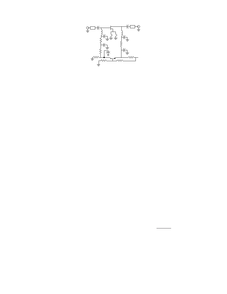
Matching Networks
The techniques for impedance
matching an enhancement mode
device are very similar to those
for matching a depletion mode
device. The only difference is in
the method of supplying gate
bias. S and Noise Parameters for
various bias conditions are listed
in this data sheet. The circuit
shown in Figure 1 shows a typical
LNA circuit normally used for
900 and 1900 MHz applications
(Consult the Agilent Technologies
website for application notes
covering specific applications).
High pass impedance matching
networks consisting of L1/C1 and
L4/C4 provide the appropriate
match for noise figure, gain, S11
and S22. The high pass structure
also provides low frequency gain
reduction which can be beneficial
from the standpoint of improving
out-of-band rejection at lower
frequencies.
INPUT
C1
C2
C3
C7
L1
R5
R6
R7
R3
R2
R1
Q2
Vdd
R4
L2
L3
L4
Q1
Zo
C4
C5
C6
OUTPUT
Figure 1. Typical ATF-54143 LNA with Passive
Biasing.
Capacitors C2 and C5 provide a
low impedance in-band RF
bypass for the matching net-
works. Resistors R3 and R4
provide a very important low
frequency termination for the
device. The resistive termination
improves low frequency stability.
Capacitors C3 and C6 provide
the low frequency RF bypass for
resistors R3 and R4. Their value
should be chosen carefully as C3
and C6 also provide a termina-
tion for low frequency mixing
products. These mixing products
are as a result of two or more in-
band signals mixing and produc-
ing third order in-band distortion
products. The low frequency or
difference mixing products are
bypassed by C3 and C6. For best
suppression of third order
distortion products based on the
CDMA 1.25 MHz signal spacing,
C3 and C6 should be 0.1
F in
value. Smaller values of capaci-
tance will not suppress the
generation of the 1.25 MHz
difference signal and as a result
will show up as poorer two tone
IP3 results.
Bias Networks
One of the major advantages of
the enhancement mode technol-
ogy is that it allows the designer
to be able to dc ground the
source leads and then merely
apply a positive voltage on the
gate to set the desired amount of
quiescent drain current Id.
Whereas a depletion mode
PHEMT pulls maximum drain
current when V
gs = 0V, an en-
hancement mode PHEMT pulls
only a small amount of leakage
current when V
gs = 0 V. Only when
V
gs is increased above Vto, the
device threshold voltage, will
drain current start to flow. At a
V
ds of 3V and a nominal Vgs of
0.6V, the drain current I
d will be
approximately 60 mA. The data
sheet suggests a minimum and
maximum V
gs over which the
desired amount of drain current
will be achieved. It is also impor-
tant to note that if the gate
terminal is left open circuited,
the device will pull some amount
of drain current due to leakage
current creating a voltage differ-
ential between the gate and
source terminals.
Passive Biasing
Passive biasing of the ATF-54143
is accomplished by the use of a
voltage divider consisting of R1
and R2. The voltage for the
divider is derived from the drain
voltage which provides a form of
voltage feedback through the use
of R3 to help keep drain current
constant. Resistor R5 (approxi-
mately 10k
) provides current
limiting for the gate of enhance-
ment mode devices such as the
ATF-54143. This is especially
important when the device is
driven to P1dB or PSAT.
Resistor R3 is calculated based
on desired Vds, Ids and available
power supply voltage.
R3 =
V
DD – V
ds
(1)
p
I
ds + IBB
V
DD is the power supply voltage.
Vds is the device drain to source
voltage.
I
ds is the desired drain current.
I
BB
is the current flowing through
the R1/R2 resistor voltage
divider network.
相关PDF资料 |
PDF描述 |
|---|---|
| ATF-54143-BLKG | C BAND, GaAs, N-CHANNEL, RF SMALL SIGNAL, HEMFET |
| ATF-54143-TR1G | C BAND, GaAs, N-CHANNEL, RF SMALL SIGNAL, HEMFET |
| ATF-54143-TR2 | C BAND, GaAs, N-CHANNEL, RF SMALL SIGNAL, HEMFET |
| ATF-54143-TR2G | C BAND, GaAs, N-CHANNEL, RF SMALL SIGNAL, HEMFET |
| ATF-541M4-TR1G | X BAND, Si, N-CHANNEL, RF SMALL SIGNAL, HEMFET |
相关代理商/技术参数 |
参数描述 |
|---|---|
| ATF-54143-BLKG | 功能描述:射频GaAs晶体管 Transistor GaAs Single Voltage RoHS:否 制造商:TriQuint Semiconductor 技术类型:pHEMT 频率:500 MHz to 3 GHz 增益:10 dB 噪声系数: 正向跨导 gFS(最大值/最小值):4 S 漏源电压 VDS: 闸/源击穿电压:- 8 V 漏极连续电流:3 A 最大工作温度:+ 150 C 功率耗散:10 W 安装风格: 封装 / 箱体: |
| ATF-54143-TR1 | 功能描述:IC TRANS E-PHEMT 2GHZ SOT-343 RoHS:否 类别:分离式半导体产品 >> RF FET 系列:- 产品目录绘图:MOSFET SOT-23-3 Pkg 标准包装:3,000 系列:- 晶体管类型:N 通道 JFET 频率:- 增益:- 电压 - 测试:- 额定电流:30mA 噪音数据:- 电流 - 测试:- 功率 - 输出:- 电压 - 额定:25V 封装/外壳:TO-236-3,SC-59,SOT-23-3 供应商设备封装:SOT-23-3(TO-236) 包装:带卷 (TR) 产品目录页面:1558 (CN2011-ZH PDF) 其它名称:MMBFJ309LT1GOSMMBFJ309LT1GOS-NDMMBFJ309LT1GOSTR |
| ATF-54143-TR1G | 功能描述:射频GaAs晶体管 Transistor GaAs Single Voltage RoHS:否 制造商:TriQuint Semiconductor 技术类型:pHEMT 频率:500 MHz to 3 GHz 增益:10 dB 噪声系数: 正向跨导 gFS(最大值/最小值):4 S 漏源电压 VDS: 闸/源击穿电压:- 8 V 漏极连续电流:3 A 最大工作温度:+ 150 C 功率耗散:10 W 安装风格: 封装 / 箱体: |
| ATF-54143-TR2 | 制造商:AGILENT 制造商全称:AGILENT 功能描述:Low Noise Enhancement Mode Pseudomorphic HEMT in a Surface Mount Plastic Package |
| ATF-54143-TR2G | 功能描述:射频GaAs晶体管 Transistor GaAs Single Voltage RoHS:否 制造商:TriQuint Semiconductor 技术类型:pHEMT 频率:500 MHz to 3 GHz 增益:10 dB 噪声系数: 正向跨导 gFS(最大值/最小值):4 S 漏源电压 VDS: 闸/源击穿电压:- 8 V 漏极连续电流:3 A 最大工作温度:+ 150 C 功率耗散:10 W 安装风格: 封装 / 箱体: |
发布紧急采购,3分钟左右您将得到回复。