- 您现在的位置:买卖IC网 > PDF目录42904 > ATF-54143-BLK (AGILENT TECHNOLOGIES INC) C BAND, GaAs, N-CHANNEL, RF SMALL SIGNAL, HEMFET PDF资料下载
参数资料
| 型号: | ATF-54143-BLK |
| 厂商: | AGILENT TECHNOLOGIES INC |
| 元件分类: | 小信号晶体管 |
| 英文描述: | C BAND, GaAs, N-CHANNEL, RF SMALL SIGNAL, HEMFET |
| 封装: | PLASTIC, SC-70, 4 PIN |
| 文件页数: | 3/17页 |
| 文件大小: | 212K |
| 代理商: | ATF-54143-BLK |
11
The values of resistors R1 and R2
are calculated with the following
formulas
R1 =
Vgs
(2)
p
I
BB
R2 =
(V
ds – V
gs) R1
(3)
p
Vgs
Example Circuit
V
DD = 5 V
Vds = 3V
Ids = 60 mA
Vgs = 0.59V
Choose I
BB to be at least 10X the
normal expected gate leakage
current. I
BB was chosen to be
2 mA for this example. Using
equations (1), (2), and (3) the
resistors are calculated as
follows
R1 = 295
R2 = 1205
R3 = 32.3
Active Biasing
Active biasing provides a means
of keeping the quiescent bias
point constant over temperature
and constant over lot to lot
variations in device dc perfor-
mance. The advantage of the
active biasing of an enhancement
mode PHEMT versus a depletion
mode PHEMT is that a negative
power source is not required. The
techniques of active biasing an
enhancement mode device are
very similar to those used to bias
a bipolar junction transistor.
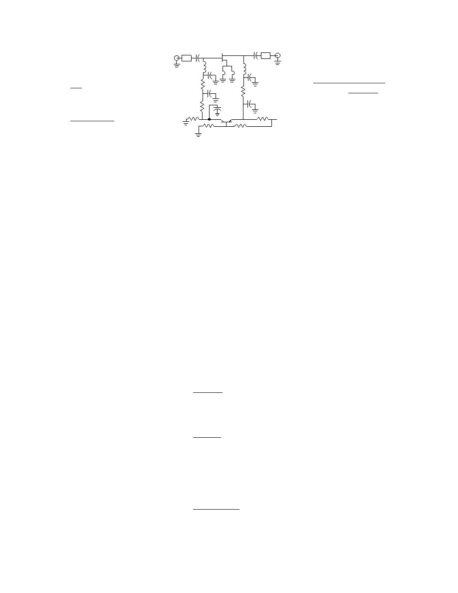
INPUT
C1
C2
C3
C7
L1
R5
R6
R7
R3
R2
R1
Q2
Vdd
R4
L2
L3
L4
Q1
Zo
C4
C5
C6
OUTPUT
Figure 2. Typical ATF-54143 LNA with
Active Biasing.
An active bias scheme is shown
in Figure 2. R1 and R2 provide a
constant voltage source at the
base of a PNP transistor at Q2.
The constant voltage at the base
of Q2 is raised by 0.7 volts at the
emitter. The constant emitter
voltage plus the regulated V
DD
supply are present across resis-
tor R3. Constant voltage across
R3 provides a constant current
supply for the drain current.
Resistors R1 and R2 are used to
set the desired Vds. The com-
bined series value of these
resistors also sets the amount of
extra current consumed by the
bias network. The equations that
describe the circuit’s operation
are as follows.
V
E = V
ds + (Ids R4)
(1)
R3 =
V
DD – V
E
(2)
p
Ids
V
B = VE – VBE
(3)
V
B =
R1
V
DD
(4)
p
R1 + R2
V
DD = I
BB (R1 + R2)
(5)
Rearranging equation (4)
provides the following formula
R2 =
R
1 (V
DD – VB)
(4A)
p
VB
and rearranging equation (5)
provides the following formula
R1 =
V
DD
(5A)
9
I
BB
(1 +
V
DD – VB
)p
V
B
Example Circuit
V
DD = 5 V
Vds = 3V
I
ds = 60 mA
R4 = 10
V
BE = 0.7 V
Equation (1) calculates the
required voltage at the emitter of
the PNP transistor based on
desired Vds and Ids through
resistor R4 to be 3.6V. Equation
(2) calculates the value of resis-
tor R3 which determines the
drain current Ids. In the example
R3 = 23.3
. Equation (3) calcu-
lates the voltage required at the
junction of resistors R1 and R2.
This voltage plus the step-up of
the base emitter junction deter-
mines the regulated Vds. Equa-
tions (4) and (5) are solved
simultaneously to determine the
value of resistors R1 and R2. In
the example R1=1450
and
R2 = 1050
. R7 is chosen to be
1k
. This resistor keeps a small
amount of current flowing
through Q2 to help maintain bias
stability. R6 is chosen to be
10k
. This value of resistance is
necessary to limit Q1 gate
current in the presence of high
RF drive level (especially when
Q1 is driven to P1dB gain com-
pression point).
相关PDF资料 |
PDF描述 |
|---|---|
| ATF-54143-BLKG | C BAND, GaAs, N-CHANNEL, RF SMALL SIGNAL, HEMFET |
| ATF-54143-TR1G | C BAND, GaAs, N-CHANNEL, RF SMALL SIGNAL, HEMFET |
| ATF-54143-TR2 | C BAND, GaAs, N-CHANNEL, RF SMALL SIGNAL, HEMFET |
| ATF-54143-TR2G | C BAND, GaAs, N-CHANNEL, RF SMALL SIGNAL, HEMFET |
| ATF-541M4-TR1G | X BAND, Si, N-CHANNEL, RF SMALL SIGNAL, HEMFET |
相关代理商/技术参数 |
参数描述 |
|---|---|
| ATF-54143-BLKG | 功能描述:射频GaAs晶体管 Transistor GaAs Single Voltage RoHS:否 制造商:TriQuint Semiconductor 技术类型:pHEMT 频率:500 MHz to 3 GHz 增益:10 dB 噪声系数: 正向跨导 gFS(最大值/最小值):4 S 漏源电压 VDS: 闸/源击穿电压:- 8 V 漏极连续电流:3 A 最大工作温度:+ 150 C 功率耗散:10 W 安装风格: 封装 / 箱体: |
| ATF-54143-TR1 | 功能描述:IC TRANS E-PHEMT 2GHZ SOT-343 RoHS:否 类别:分离式半导体产品 >> RF FET 系列:- 产品目录绘图:MOSFET SOT-23-3 Pkg 标准包装:3,000 系列:- 晶体管类型:N 通道 JFET 频率:- 增益:- 电压 - 测试:- 额定电流:30mA 噪音数据:- 电流 - 测试:- 功率 - 输出:- 电压 - 额定:25V 封装/外壳:TO-236-3,SC-59,SOT-23-3 供应商设备封装:SOT-23-3(TO-236) 包装:带卷 (TR) 产品目录页面:1558 (CN2011-ZH PDF) 其它名称:MMBFJ309LT1GOSMMBFJ309LT1GOS-NDMMBFJ309LT1GOSTR |
| ATF-54143-TR1G | 功能描述:射频GaAs晶体管 Transistor GaAs Single Voltage RoHS:否 制造商:TriQuint Semiconductor 技术类型:pHEMT 频率:500 MHz to 3 GHz 增益:10 dB 噪声系数: 正向跨导 gFS(最大值/最小值):4 S 漏源电压 VDS: 闸/源击穿电压:- 8 V 漏极连续电流:3 A 最大工作温度:+ 150 C 功率耗散:10 W 安装风格: 封装 / 箱体: |
| ATF-54143-TR2 | 制造商:AGILENT 制造商全称:AGILENT 功能描述:Low Noise Enhancement Mode Pseudomorphic HEMT in a Surface Mount Plastic Package |
| ATF-54143-TR2G | 功能描述:射频GaAs晶体管 Transistor GaAs Single Voltage RoHS:否 制造商:TriQuint Semiconductor 技术类型:pHEMT 频率:500 MHz to 3 GHz 增益:10 dB 噪声系数: 正向跨导 gFS(最大值/最小值):4 S 漏源电压 VDS: 闸/源击穿电压:- 8 V 漏极连续电流:3 A 最大工作温度:+ 150 C 功率耗散:10 W 安装风格: 封装 / 箱体: |
发布紧急采购,3分钟左右您将得到回复。