- 您现在的位置:买卖IC网 > PDF目录42904 > ATF-541M4-BLK (AGILENT TECHNOLOGIES INC) X BAND, Si, N-CHANNEL, RF SMALL SIGNAL, HEMFET PDF资料下载
参数资料
| 型号: | ATF-541M4-BLK |
| 厂商: | AGILENT TECHNOLOGIES INC |
| 元件分类: | 小信号晶体管 |
| 英文描述: | X BAND, Si, N-CHANNEL, RF SMALL SIGNAL, HEMFET |
| 封装: | 1.4 MM X 1.2 MM, 0.7 MM HEIGHT, MINIATURE PACKAGE-4 |
| 文件页数: | 2/16页 |
| 文件大小: | 166K |
| 代理商: | ATF-541M4-BLK |
10
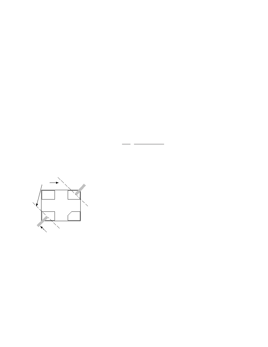
S and Noise Parameter Measurements
The position of the reference
planes used for the measurement
of both S and Noise Parameter
measurements is shown in Figure
20. The reference plane can be
described as being at the center
of both the gate and drain pads.
S and noise parameters are
measured with a 50 ohm
microstrip test fixture made with
a 0.010" thickness aluminum
substrate. Both source leads are
connected directly to ground via
a 0.010" thickness metal rib
which provides a very low
inductance path to ground for
both source leads. The induc-
tance associated with the addi-
tion of printed circuit board
plated through holes and source
bypass capacitors must be added
to the computer circuit simula-
tion to properly model the effect
of grounding the source leads in
a typical amplifier design.
Gate
Pin 2
Source
Pin 3
Drain
Pin 4
Source
Pin 1
Reference
Plane
Microstrip
Transmission Lines
Sx
Figure 20.
Noise Parameter Applications
Information
The Fmin values are based on a
set of 16 noise figure measure-
ments made at 16 different
impedances using an ATN NP5
test system. From these measure-
ments, a true Fmin is calculated.
Fmin represents the true mini-
mum noise figure of the device
when the device is presented
with an impedance matching
network that transforms the
source impedance, typically 50
,
to an impedance represented by
the reflection coefficient
Γ
o. The
designer must design a matching
network that will present
Γ
o to
the device with minimal associ-
ated circuit losses. The noise
figure of the completed amplifier
is equal to the noise figure of the
device plus the losses of the
matching network preceding the
device. The noise figure of the
device is equal to Fmin only
when the device is presented
with
Γ
o. If the reflection coeffi-
cient of the matching network is
other than
Γ
o, then the noise
figure of the device will be
greater than Fmin based on the
following equation.
NF = Fmin + 4 Rn
|
Γ
s – Γo |
2
Zo (|1 +
Γo|2)(1 - |Γs|2)
Where Rn/Zo is the normalized
noise resistance,
Γ
o is the opti-
mum reflection coefficient
required to produce Fmin and
Γ
s
is the reflection coefficient of the
source impedance actually
presented to the device.
The losses of the matching
networks are non-zero and they
will also add to the noise figure
of the device creating a higher
amplifier noise figure. The losses
of the matching networks are
related to the Q of the compo-
nents and associated printed
circuit board loss.
Γ
o is typically
fairly low at higher frequencies
and increases as frequency is
lowered. Larger gate width
devices will typically have a
lower
Γ
o as compared to nar-
rower gate width devices. Typi-
cally for FETs , the higher
Γ
o
usually infers that an impedance
much higher than 50
is re-
quired for the device to produce
Fmin. At VHF frequencies and
even lower L Band frequencies,
the required impedance can be in
the vicinity of several thousand
ohms. Matching to such a high
impedance requires very hi-Q
components in order to minimize
circuit losses. As an example at
900 MHz, when airwwound coils
(Q>100)are used for matching
networks, the loss can still be up
to 0.25 dB which will add di-
rectly to the noise figure of the
device. Using muiltilayer molded
inductors with Qs in the 30 to 50
range results in additional loss
over the airwound coil. Losses as
high as 0.5 dB or greater add to
the typical 0.15 dB Fmin of the
device creating an amplifier
noise figure of nearly 0.65 dB.
SMT Assembly
The package can be soldered
using either lead-bearing or lead-
free alloys (higher peak tempera-
tures). Reliable assembly of
surface mount components is a
complex process that involves
many material, process, and
equipment factors, including:
method of heating (e.g. IR or
vapor phase reflow, wave solder-
ing, etc) circuit board material,
conductor thickness and pattern,
type of solder alloy, and the
thermal conductivity and ther-
mal mass of components. Compo-
nents with a low mass, such as
the Minipak 1412 package, will
reach solder reflow temperatures
faster than those with a greater
mass.
The recommended leaded solder
time-temperature profile is
shown in Figure 21. This profile
is representative of an IR reflow
type of surface mount assembly
process. After ramping up from
room temperature, the circuit
board with components attached
to it (held in place with solder
paste) passes through one or
more preheat zones. The preheat
zones increase the temperature
of the board and components to
prevent thermal shock and begin
evaporating solvents from the
solder paste. The reflow zone
相关PDF资料 |
PDF描述 |
|---|---|
| ATF-541M4-TR1 | X BAND, Si, N-CHANNEL, RF SMALL SIGNAL, HEMFET |
| ATF-541M4-BLKG | X BAND, Si, N-CHANNEL, RF SMALL SIGNAL, HEMFET |
| ATF-541M4-TR2 | X BAND, Si, N-CHANNEL, RF SMALL SIGNAL, HEMFET |
| ATF-541M4-TR2 | C BAND, Si, N-CHANNEL, RF SMALL SIGNAL, HEMFET |
| ATF-541M4-BLK | C BAND, Si, N-CHANNEL, RF SMALL SIGNAL, HEMFET |
相关代理商/技术参数 |
参数描述 |
|---|---|
| ATF-541M4-BLK | 制造商:Avago Technologies 功能描述:RF BIPOLAR TRANSISTOR |
| ATF-541M4-TR1 | 功能描述:射频GaAs晶体管 Transistor GaAs Single Voltage RoHS:否 制造商:TriQuint Semiconductor 技术类型:pHEMT 频率:500 MHz to 3 GHz 增益:10 dB 噪声系数: 正向跨导 gFS(最大值/最小值):4 S 漏源电压 VDS: 闸/源击穿电压:- 8 V 漏极连续电流:3 A 最大工作温度:+ 150 C 功率耗散:10 W 安装风格: 封装 / 箱体: |
| ATF-541M4-TR2 | 功能描述:射频GaAs晶体管 Transistor GaAs Single Voltage RoHS:否 制造商:TriQuint Semiconductor 技术类型:pHEMT 频率:500 MHz to 3 GHz 增益:10 dB 噪声系数: 正向跨导 gFS(最大值/最小值):4 S 漏源电压 VDS: 闸/源击穿电压:- 8 V 漏极连续电流:3 A 最大工作温度:+ 150 C 功率耗散:10 W 安装风格: 封装 / 箱体: |
| ATF55143 | 制造商:AGILENT 制造商全称:AGILENT 功能描述:Agilent ATF-55143 Low Noise Enhancement Mode Pseudomorphic HEMT in a Surface Mount Plastic Package |
| ATF-55143 | 制造商:Avago Technologies 功能描述:MOSFET RF HEMT SOT-343 |
发布紧急采购,3分钟左右您将得到回复。