- 您现在的位置:买卖IC网 > PDF目录11800 > ATMEGA649V-8AUR (Atmel)IC AVR MCU FLASH 64K 1.8V 64TQFP PDF资料下载
参数资料
| 型号: | ATMEGA649V-8AUR |
| 厂商: | Atmel |
| 文件页数: | 138/146页 |
| 文件大小: | 0K |
| 描述: | IC AVR MCU FLASH 64K 1.8V 64TQFP |
| 产品培训模块: | megaAVR Introduction |
| 标准包装: | 1,000 |
| 系列: | AVR® ATmega |
| 核心处理器: | AVR |
| 芯体尺寸: | 8-位 |
| 速度: | 8MHz |
| 连通性: | SPI,UART/USART,USI |
| 外围设备: | 欠压检测/复位,LCD,POR,PWM,WDT |
| 输入/输出数: | 53 |
| 程序存储器容量: | 64KB(32K x 16) |
| 程序存储器类型: | 闪存 |
| EEPROM 大小: | 2K x 8 |
| RAM 容量: | 4K x 8 |
| 电压 - 电源 (Vcc/Vdd): | 1.8 V ~ 5.5 V |
| 数据转换器: | A/D 8x10b |
| 振荡器型: | 内部 |
| 工作温度: | -40°C ~ 85°C |
| 封装/外壳: | 64-TQFP |
| 包装: | 带卷 (TR) |
| 其它名称: | ATMEGA649V-8AUR-ND ATMEGA649V-8AURTR |
第1页第2页第3页第4页第5页第6页第7页第8页第9页第10页第11页第12页第13页第14页第15页第16页第17页第18页第19页第20页第21页第22页第23页第24页第25页第26页第27页第28页第29页第30页第31页第32页第33页第34页第35页第36页第37页第38页第39页第40页第41页第42页第43页第44页第45页第46页第47页第48页第49页第50页第51页第52页第53页第54页第55页第56页第57页第58页第59页第60页第61页第62页第63页第64页第65页第66页第67页第68页第69页第70页第71页第72页第73页第74页第75页第76页第77页第78页第79页第80页第81页第82页第83页第84页第85页第86页第87页第88页第89页第90页第91页第92页第93页第94页第95页第96页第97页第98页第99页第100页第101页第102页第103页第104页第105页第106页第107页第108页第109页第110页第111页第112页第113页第114页第115页第116页第117页第118页第119页第120页第121页第122页第123页第124页第125页第126页第127页第128页第129页第130页第131页第132页第133页第134页第135页第136页第137页当前第138页第139页第140页第141页第142页第143页第144页第145页第146页
65
2552K–AVR–04/11
ATmega329/3290/649/6490
ing inputs should be avoided to reduce current consumption in all other modes where the digital
inputs are enabled (Reset, Active mode and Idle mode).
The simplest method to ensure a defined level of an unused pin, is to enable the internal pull-up.
In this case, the pull-up will be disabled during reset. If low power consumption during reset is
important, it is recommended to use an external pull-up or pull-down. Connecting unused pins
directly to V
CC or GND is not recommended, since this may cause excessive currents if the pin is
accidentally configured as an output.
13.3
Alternate Port Functions
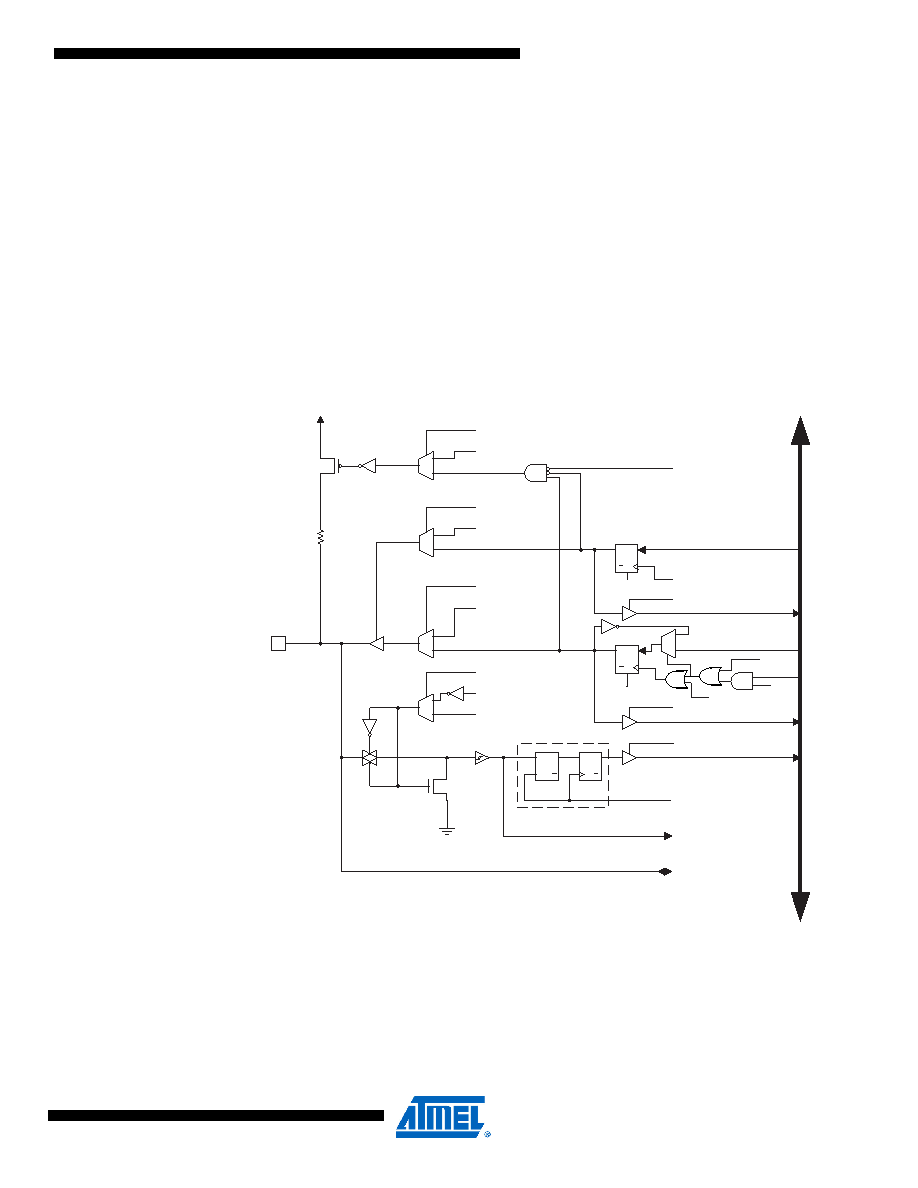
Most port pins have alternate functions in addition to being general digital I/Os. Figure 13-5
shows how the port pin control signals from the simplified Figure 13-2 can be overridden by
alternate functions. The overriding signals may not be present in all port pins, but the figure
serves as a generic description applicable to all port pins in the AVR microcontroller family.
Figure 13-5. Alternate Port Functions(1)
Note:
1. WRx, WPx, WDx, RRx, RPx, and RDx are common to all pins within the same port. clkI/O,
SLEEP, and PUD are common to all ports. All other signals are unique for each pin.
clk
RPx
RRx
WRx
RDx
WDx
PUD
SYNCHRONIZER
WDx:
WRITE DDRx
WRx:
WRITE PORTx
RRx:
READ PORTx REGISTER
RPx:
READ PORTx PIN
PUD:
PULLUP DISABLE
clk
I/O:
I/O CLOCK
RDx:
READ DDRx
D
L
Q
SET
CLR
0
1
0
1
0
1
DIxn
AIOxn
DIEOExn
PVOVxn
PVOExn
DDOVxn
DDOExn
PUOExn
PUOVxn
PUOExn:
Pxn PULL-UP OVERRIDE ENABLE
PUOVxn:
Pxn PULL-UP OVERRIDE VALUE
DDOExn:
Pxn DATA DIRECTION OVERRIDE ENABLE
DDOVxn:
Pxn DATA DIRECTION OVERRIDE VALUE
PVOExn:
Pxn PORT VALUE OVERRIDE ENABLE
PVOVxn:
Pxn PORT VALUE OVERRIDE VALUE
DIxn:
DIGITAL INPUT PIN n ON PORTx
AIOxn:
ANALOG INPUT/OUTPUT PIN n ON PORTx
RESET
Q
D
CLR
Q
D
CLR
Q
D
CLR
PINxn
PORTxn
DDxn
D
ATA
B
U
S
0
1
DIEOVxn
SLEEP
DIEOExn: Pxn DIGITAL INPUT-ENABLE OVERRIDE ENABLE
DIEOVxn: Pxn DIGITAL INPUT-ENABLE OVERRIDE VALUE
SLEEP:
SLEEP CONTROL
Pxn
I/O
0
1
PTOExn
WPx
PTOExn:
Pxn, PORT TOGGLE OVERRIDE ENABLE
WPx:
WRITE PINx
相关PDF资料 |
PDF描述 |
|---|---|
| ATMEGA649V-8MUR | MCU AVR 64KB FLASH 8MHZ 64QFN |
| D38999/20JA98PN | CONN RCPT 3POS WALL MNT W/PINS |
| V48A15E500BF3 | CONVERTER MOD DC/DC 15V 500W |
| MS27508E14F37S | CONN RCPT 37POS BOX MNT W/SCKT |
| V48A15E500BF2 | CONVERTER MOD DC/DC 15V 500W |
相关代理商/技术参数 |
参数描述 |
|---|---|
| ATmega649V-8MI | 功能描述:8位微控制器 -MCU AVR 64K FLASH 2K EE 4K SRAM ADC LCD RoHS:否 制造商:Silicon Labs 核心:8051 处理器系列:C8051F39x 数据总线宽度:8 bit 最大时钟频率:50 MHz 程序存储器大小:16 KB 数据 RAM 大小:1 KB 片上 ADC:Yes 工作电源电压:1.8 V to 3.6 V 工作温度范围:- 40 C to + 105 C 封装 / 箱体:QFN-20 安装风格:SMD/SMT |
| ATmega649V-8MU | 功能描述:8位微控制器 -MCU AVR 64K FLASH 2K EE 4K SRAM ADC LCD RoHS:否 制造商:Silicon Labs 核心:8051 处理器系列:C8051F39x 数据总线宽度:8 bit 最大时钟频率:50 MHz 程序存储器大小:16 KB 数据 RAM 大小:1 KB 片上 ADC:Yes 工作电源电压:1.8 V to 3.6 V 工作温度范围:- 40 C to + 105 C 封装 / 箱体:QFN-20 安装风格:SMD/SMT |
| ATMEGA649V-8MUR | 功能描述:8位微控制器 -MCU AVR 64KB FLSH 2KB EE 4KB SRAM LCD8MHz1.8V RoHS:否 制造商:Silicon Labs 核心:8051 处理器系列:C8051F39x 数据总线宽度:8 bit 最大时钟频率:50 MHz 程序存储器大小:16 KB 数据 RAM 大小:1 KB 片上 ADC:Yes 工作电源电压:1.8 V to 3.6 V 工作温度范围:- 40 C to + 105 C 封装 / 箱体:QFN-20 安装风格:SMD/SMT |
| ATMEGA64A-AN | 功能描述:8位微控制器 -MCU 16MHz 105C RoHS:否 制造商:Silicon Labs 核心:8051 处理器系列:C8051F39x 数据总线宽度:8 bit 最大时钟频率:50 MHz 程序存储器大小:16 KB 数据 RAM 大小:1 KB 片上 ADC:Yes 工作电源电压:1.8 V to 3.6 V 工作温度范围:- 40 C to + 105 C 封装 / 箱体:QFN-20 安装风格:SMD/SMT |
| ATMEGA64A-ANR | 功能描述:8位微控制器 -MCU 16MHz 105C RoHS:否 制造商:Silicon Labs 核心:8051 处理器系列:C8051F39x 数据总线宽度:8 bit 最大时钟频率:50 MHz 程序存储器大小:16 KB 数据 RAM 大小:1 KB 片上 ADC:Yes 工作电源电压:1.8 V to 3.6 V 工作温度范围:- 40 C to + 105 C 封装 / 箱体:QFN-20 安装风格:SMD/SMT |
发布紧急采购,3分钟左右您将得到回复。