参数资料
| 型号: | ATTINY26L-8PU |
| 厂商: | Atmel |
| 文件页数: | 108/169页 |
| 文件大小: | 0K |
| 描述: | IC MCU AVR 2K 5V 8MHZ 20-DIP |
| 产品培训模块: | MCU Product Line Introduction tinyAVR Introduction |
| 标准包装: | 18 |
| 系列: | AVR® ATtiny |
| 核心处理器: | AVR |
| 芯体尺寸: | 8-位 |
| 速度: | 8MHz |
| 连通性: | USI |
| 外围设备: | 欠压检测/复位,POR,PWM,WDT |
| 输入/输出数: | 16 |
| 程序存储器容量: | 2KB(1K x 16) |
| 程序存储器类型: | 闪存 |
| EEPROM 大小: | 128 x 8 |
| RAM 容量: | 128 x 8 |
| 电压 - 电源 (Vcc/Vdd): | 2.7 V ~ 5.5 V |
| 数据转换器: | A/D 11x10b |
| 振荡器型: | 内部 |
| 工作温度: | -40°C ~ 85°C |
| 封装/外壳: | 20-DIP(0.300",7.62mm) |
| 包装: | 管件 |
| 产品目录页面: | 612 (CN2011-ZH PDF) |
| 配用: | ATSTK600-RC08-ND - STK600 ROUTING CARD AVR ATSTK600-ND - DEV KIT FOR AVR/AVR32 ATAVRISP2-ND - PROGRAMMER AVR IN SYSTEM ATSTK505-ND - ADAPTER KIT FOR 14PIN AVR MCU |
| 其它名称: | ATTINY26L-8PJ ATTINY26L-8PJ-ND |
第1页第2页第3页第4页第5页第6页第7页第8页第9页第10页第11页第12页第13页第14页第15页第16页第17页第18页第19页第20页第21页第22页第23页第24页第25页第26页第27页第28页第29页第30页第31页第32页第33页第34页第35页第36页第37页第38页第39页第40页第41页第42页第43页第44页第45页第46页第47页第48页第49页第50页第51页第52页第53页第54页第55页第56页第57页第58页第59页第60页第61页第62页第63页第64页第65页第66页第67页第68页第69页第70页第71页第72页第73页第74页第75页第76页第77页第78页第79页第80页第81页第82页第83页第84页第85页第86页第87页第88页第89页第90页第91页第92页第93页第94页第95页第96页第97页第98页第99页第100页第101页第102页第103页第104页第105页第106页第107页当前第108页第109页第110页第111页第112页第113页第114页第115页第116页第117页第118页第119页第120页第121页第122页第123页第124页第125页第126页第127页第128页第129页第130页第131页第132页第133页第134页第135页第136页第137页第138页第139页第140页第141页第142页第143页第144页第145页第146页第147页第148页第149页第150页第151页第152页第153页第154页第155页第156页第157页第158页第159页第160页第161页第162页第163页第164页第165页第166页第167页第168页第169页
43
1477K–AVR–08/10
ATtiny26(L)
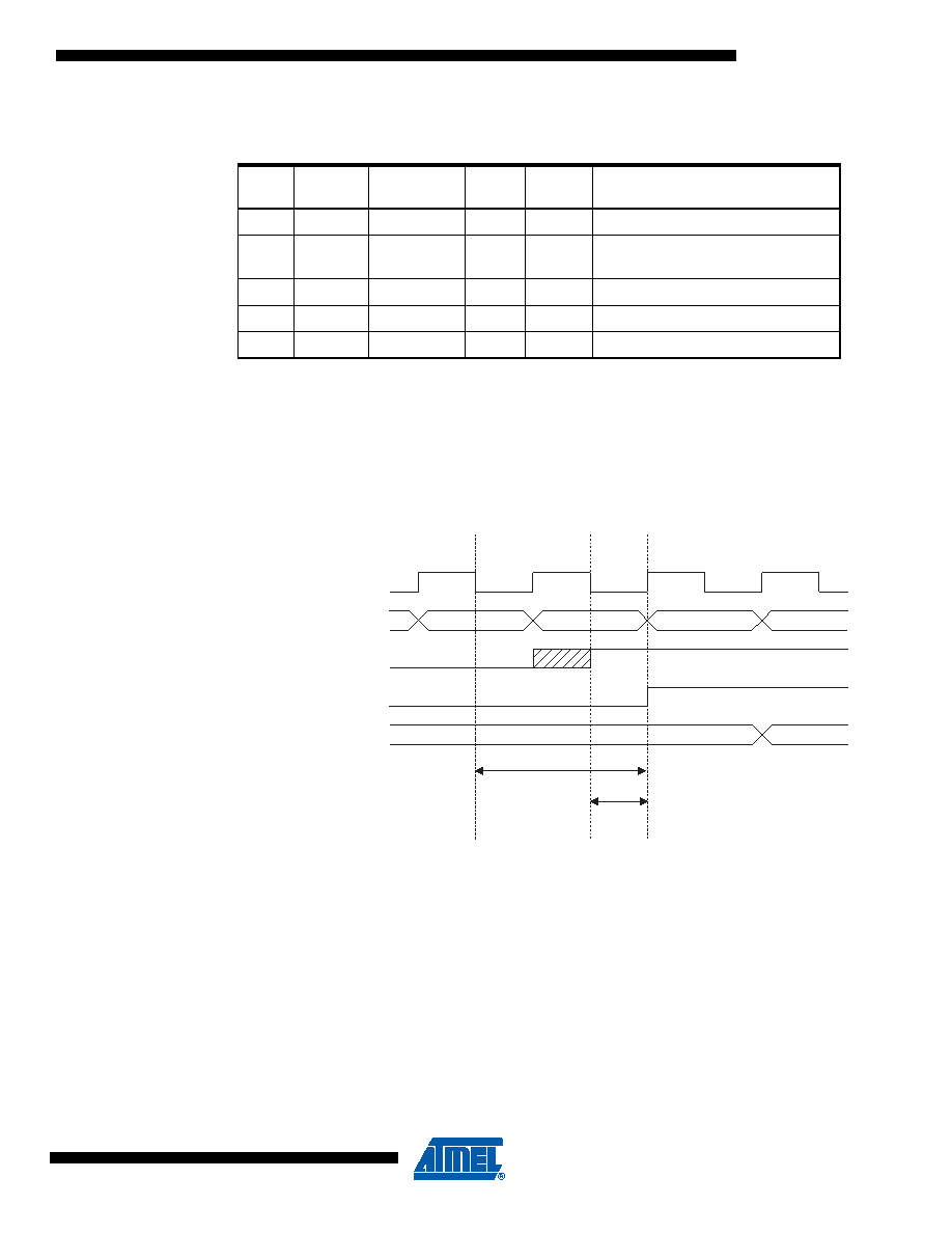
Table 21 summarizes the control signals for the pin value.
Reading the Pin Value
Independent of the setting of Data Direction bit DDxn, the port pin can be read through the
PINxn Register Bit. As shown in Figure 32, the PINxn Register bit and the preceding latch con-
stitute a synchronizer. This is needed to avoid metastability if the physical pin changes value
near the edge of the internal clock, but it also introduces a delay. Figure 33 shows a timing dia-
gram of the synchronization when reading an externally applied pin value. The maximum and
minimum propagation delays are denoted tpd,max and tpd,min respectively.
Figure 33. Synchronization when Reading an Externally Applied Pin Value
Consider the clock period starting shortly after the first falling edge of the system clock. The latch
is closed when the clock is low, and goes transparent when the clock is high, as indicated by the
shaded region of the “SYNC LATCH” signal. The signal value is latched when the system clock
goes low. It is clocked into the PINxn Register at the succeeding positive clock edge. As indi-
cated by the two arrows tpd,max and tpd,min, a single signal transition on the pin will be delayed
between and 1 system clock period depending upon the time of assertion.
When reading back a software assigned pin value, a nop instruction must be inserted as indi-
cated in Figure 34. The out instruction sets the “SYNC LATCH” signal at the positive edge of the
clock. In this case, the delay tpd through the synchronizer is one system clock period.
Table 21. Port Pin Configurations
DDxn
PORTxn
PUD
(in MCUCR)
I/O
Pull-up
Comment
0
X
Input
No
Tri-state (Hi-Z)
0
1
0
Input
Yes
Pxn will source current if ext. pulled
low
0
1
Input
No
Tri-state (Hi-Z)
1
0
X
Output
No
Output Low (Sink)
1
X
Output
No
Output High (Source)
XXX
in r17, PINx
0x00
0xFF
INSTRUCTIONS
SYNC LATCH
PINxn
r17
XXX
SYSTEM CLK
tpd, max
tpd, min
相关PDF资料 |
PDF描述 |
|---|---|
| ATTINY28V-1AUR | IC MCU AVR 2K 1.2MHZ 1.8V 32TQFP |
| ATTINY4313-MMH | IC MCU AVR 4K FLASH 20QFN |
| ATTINY43U-SUR | MCU AVR 4KB FLASH 8MHZ 20SOIC |
| ATTINY44A-MFR | MCU AVR 4KB FLASH 20MHZ 20QFN |
| ATTINY48-AUR | MCU AVR 4KB FLASH 12MHZ 32TQFP |
相关代理商/技术参数 |
参数描述 |
|---|---|
| ATTINY26L-8SC | 功能描述:8位微控制器 -MCU AVR 2K FLSH 128B EE 128B SRAM ADC 3V RoHS:否 制造商:Silicon Labs 核心:8051 处理器系列:C8051F39x 数据总线宽度:8 bit 最大时钟频率:50 MHz 程序存储器大小:16 KB 数据 RAM 大小:1 KB 片上 ADC:Yes 工作电源电压:1.8 V to 3.6 V 工作温度范围:- 40 C to + 105 C 封装 / 箱体:QFN-20 安装风格:SMD/SMT |
| ATTINY26L-8SI | 功能描述:8位微控制器 -MCU AVR 2K FLSH 128B EE 128B SRAM ADC 3V RoHS:否 制造商:Silicon Labs 核心:8051 处理器系列:C8051F39x 数据总线宽度:8 bit 最大时钟频率:50 MHz 程序存储器大小:16 KB 数据 RAM 大小:1 KB 片上 ADC:Yes 工作电源电压:1.8 V to 3.6 V 工作温度范围:- 40 C to + 105 C 封装 / 箱体:QFN-20 安装风格:SMD/SMT |
| ATTINY26L-8SI SL383 | 制造商:Atmel Corporation 功能描述:MCU 8-bit ATtiny AVR RISC 2KB Flash 3.3V/5V 20-Pin SOIC W T/R |
| ATtiny26L-8SU | 功能描述:8位微控制器 -MCU 2kB Flash 128B EE 128B SRAM RoHS:否 制造商:Silicon Labs 核心:8051 处理器系列:C8051F39x 数据总线宽度:8 bit 最大时钟频率:50 MHz 程序存储器大小:16 KB 数据 RAM 大小:1 KB 片上 ADC:Yes 工作电源电压:1.8 V to 3.6 V 工作温度范围:- 40 C to + 105 C 封装 / 箱体:QFN-20 安装风格:SMD/SMT |
| ATTINY26L-8SUR | 功能描述:8位微控制器 -MCU 2K FL 128B EE 128B SRAM ADC 8MHZ IND 3V RoHS:否 制造商:Silicon Labs 核心:8051 处理器系列:C8051F39x 数据总线宽度:8 bit 最大时钟频率:50 MHz 程序存储器大小:16 KB 数据 RAM 大小:1 KB 片上 ADC:Yes 工作电源电压:1.8 V to 3.6 V 工作温度范围:- 40 C to + 105 C 封装 / 箱体:QFN-20 安装风格:SMD/SMT |
发布紧急采购,3分钟左右您将得到回复。