参数资料
| 型号: | BD9011EKN-E2 |
| 厂商: | Rohm Semiconductor |
| 文件页数: | 14/30页 |
| 文件大小: | 0K |
| 描述: | IC REG CTRLR BST PWM 36-HQFN |
| 标准包装: | 1 |
| PWM 型: | 控制器 |
| 输出数: | 2 |
| 频率 - 最大: | 550kHz |
| 电源电压: | 3.9 V ~ 30 V |
| 降压: | 是 |
| 升压: | 是 |
| 回扫: | 无 |
| 反相: | 无 |
| 倍增器: | 无 |
| 除法器: | 无 |
| Cuk: | 无 |
| 隔离: | 无 |
| 工作温度: | -40°C ~ 105°C |
| 封装/外壳: | 36-TQFN 裸露焊盘 |
| 包装: | 标准包装 |
| 产品目录页面: | 1372 (CN2011-ZH PDF) |
| 其它名称: | BD9011EKN-E2DKR |
第1页第2页第3页第4页第5页第6页第7页第8页第9页第10页第11页第12页第13页当前第14页第15页第16页第17页第18页第19页第20页第21页第22页第23页第24页第25页第26页第27页第28页第29页第30页
�� �
�
�●� Operation� notes�
�1� )� Absolute� maximum� ratings�
�Exceeding� the� absolute� maximum� ratings� for� supply� voltage,� operating� temperature� or� other� parameters� can� damage� or�
�destroy� the� IC.� When� this� occurs,� it� is� impossible� to� identify� the� source� of� the� damage� as� a� short� circuit,� open� circuit,� etc.�
�Therefore,� if� any� special� mode� is� being� considered� with� values� expected� to� exceed� absolute� maximum� ratings,� consider�
�taking� physical� safety� measures� to� protect� the� circuits,� such� as� adding� fuses.�
�2� )� GND� electric� potential�
�Keep� the� GND� terminal� potential� at� the� lowest� (minimum)� potential� under� any� operating� condition.�
�3� )� Thermal� design�
�Be� sure� that� the� thermal� design� allows� sufficient� margin� for� power� dissipation� (Pd)� under� actual� operating� conditions.�
�4� )� Inter-pin� shorts� and� mounting� errors�
�Use� caution� when� positioning� the� IC� for� mounting� on� printed� surface� boards.� Connection� errors� may� result� in� damage� or�
�destruction� of� the� IC.� The� IC� can� also� be� damaged� when� foreign� substances� short� output� pins� together,� or� cause� shorts�
�between� the� power� supply� and� GND.�
�5� )� Operation� in� strong� electromagnetic� fields�
�Use� caution� when� operating� in� the� presence� of� strong� electromagnetic� fields,� as� this� may� cause� the� IC� to� malfunction.�
�6� )� Testing� on� application� boards�
�Connecting� a� capacitor� to� a� low� impedance� pin� for� testing� on� an� application� board� may� subject� the� IC� to� stress.� Be� sure� to�
�discharge� the� capacitors� after� every� test� process� or� step.� Always� turn� the� IC� power� supply� off� before� connecting� it� to� or�
�removing� it� from� any� of� the� apparatus� used� during� the� testing� process.� In� addition,� ground� the� IC� during� all� steps� in� the�
�assembly� process,� and� take� similar� antistatic� precautions� when� transporting� or� storing� the� IC.�
�7)� The� output� FET�
�The� shoot-through� may� happen� when� the� input� parasitic� capacitance� of� FET� is� extremely� big� or� the� Duty� ratio� is� less� than�
�or� equal� to� 10%.� Less� than� or� equal� to� 1000pF� input� parasitic� capacitance� is� recommended.� Please� confirm� operation� on�
�the� actual� application� since� this� character� is� affected� by� PCB� layout� and� components.�
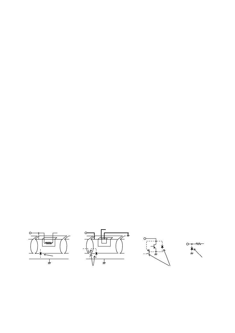
�8� )� This� monolithic� IC� contains� P+� isolation� and� P� substrate� layers� between� adjacent� elements� in� order� to� keep� them� isolated.�
�P-N� junctions� are� formed� at� the� intersection� of� these� P� layers� with� the� N� layers� of� other� elements,� creating� a� parasitic� diode�
�or� transistor.� Relations� between� each� potential� may� form� as� shown� in� the� example� below,� where� a� resistor� and� transistor�
�are� connected� to� a� pin:�
�○�
�○�
�With� the� resistor,� when� GND� >� Pin� A,� and� with� the� transistor� (NPN),� when� GND� >� Pin� B:�
�The� P-N� junction� operates� as� a� parasitic� diode�
�With� the� transistor� (NPN),� when� GND� >� Pin� B:�
�The� P-N� junction� operates� as� a� parasitic� transistor� by� interacting� with� the� N� layers� of� elements� in� proximity� to� the�
�parasitic� diode� described� above.�
�Parasitic� diodes� inevitably� occur� in� the� structure� of� the� IC.� Their� operation� can� result� in� mutual� interference� between� circuits,�
�and� can� cause� malfunctions,� and,� in� turn,� physical� damage� or� destruction.� Therefore,� do� not� employ� any� of� the� methods�
�under� which� parasitic� diodes� can� operate,� such� as� applying� a� voltage� to� an� input� pin� lower� than� the� (P� substrate)� GND.�
�Resistor�
�Transistor� (� NPN� )�
�(PINA)�
�(PINB)�
�C�
�B�
�E�
�(PINB)�
�(PINA)�
�P�
�+�
�P�
�P�
�+�
�P�
�+�
�P�
�P�
�+�
�B�
�C�
�N�
�P�
�N�
�Parasitic� element�
�GND�
�N�
�N�
�P� substrate�
�GND�
�N�
�E�
�GND�
�Parasitic� element�
�Parasitic� element� or� transistor�
�Parasitic� element� or� transistor�
�Fig-37�
�Fig-38�
�Fig-39�
�Fig-40�
�9� )� GND� wiring� pattern�
�When� both� a� small-signal� GND� and� high� current� GND� are� present,� single-point� grounding� (at� the� set� standard� point)� is�
�recommended,� in� order� to� separate� the� small-signal� and� high� current� patterns,� and� to� be� sure� voltage� changes� stemming�
�from� the� wiring� resistance� and� high� current� do� not� cause� any� voltage� change� in� the� small-signal� GND.� In� the� same� way,� care�
�must� be� taken� to� avoid� wiring� pattern� fluctuations� in� any� connected� external� component� GND.�
�14/29�
�相关PDF资料 |
PDF描述 |
|---|---|
| HBC36DRTH-S13 | CONN EDGECARD 72POS .100 EXTEND |
| RBB60DHFD | CONN EDGECARD 120POS .050 SMD |
| LTC3803ES6#TRMPBF | IC REG CTRLR FLYBK PWM TSOT23-6 |
| RSC35DRXS | CONN EDGECARD 70POS DIP .100 SLD |
| HBC30DRYN | CONN EDGECARD 60POS DIP .100 SLD |
相关代理商/技术参数 |
参数描述 |
|---|---|
| BD9011KV | 制造商:ROHM 制造商全称:Rohm 功能描述:Dual Synchronous DC/DC converter controller |
| BD9011KV-E2 | 功能描述:DC/DC 开关控制器 Step Down; 2 Outputs RoHS:否 制造商:Texas Instruments 输入电压:6 V to 100 V 开关频率: 输出电压:1.215 V to 80 V 输出电流:3.5 A 输出端数量:1 最大工作温度:+ 125 C 安装风格: 封装 / 箱体:CPAK |
| BD9012KV | 制造商:ROHM 制造商全称:Rohm 功能描述:Dual-output, high voltage, high-efficiency step-down switching controller |
| BD9012KV-E2 | 功能描述:开关变换器、稳压器与控制器 Step Down; 2 Outputs RoHS:否 制造商:Texas Instruments 输出电压:1.2 V to 10 V 输出电流:300 mA 输出功率: 输入电压:3 V to 17 V 开关频率:1 MHz 工作温度范围: 安装风格:SMD/SMT 封装 / 箱体:WSON-8 封装:Reel |
| BD9013KV-E2 | 功能描述:DC/DC 开关控制器 Step Down; 2 Outputs RoHS:否 制造商:Texas Instruments 输入电压:6 V to 100 V 开关频率: 输出电压:1.215 V to 80 V 输出电流:3.5 A 输出端数量:1 最大工作温度:+ 125 C 安装风格: 封装 / 箱体:CPAK |
发布紧急采购,3分钟左右您将得到回复。