参数资料
| 型号: | BD9011EKN-E2 |
| 厂商: | Rohm Semiconductor |
| 文件页数: | 15/30页 |
| 文件大小: | 0K |
| 描述: | IC REG CTRLR BST PWM 36-HQFN |
| 标准包装: | 1 |
| PWM 型: | 控制器 |
| 输出数: | 2 |
| 频率 - 最大: | 550kHz |
| 电源电压: | 3.9 V ~ 30 V |
| 降压: | 是 |
| 升压: | 是 |
| 回扫: | 无 |
| 反相: | 无 |
| 倍增器: | 无 |
| 除法器: | 无 |
| Cuk: | 无 |
| 隔离: | 无 |
| 工作温度: | -40°C ~ 105°C |
| 封装/外壳: | 36-TQFN 裸露焊盘 |
| 包装: | 标准包装 |
| 产品目录页面: | 1372 (CN2011-ZH PDF) |
| 其它名称: | BD9011EKN-E2DKR |
第1页第2页第3页第4页第5页第6页第7页第8页第9页第10页第11页第12页第13页第14页当前第15页第16页第17页第18页第19页第20页第21页第22页第23页第24页第25页第26页第27页第28页第29页第30页
�� �
�
�10� )� In� some� application� and� process� testing,� Vcc� and� pin� potential� may� be� reversed,� possibly� causing� internal� circuit� or� element�
�damage.� For� example,� when� the� external� capacitor� is� charged,� the� electric� charge� can� cause� a� Vcc� short� circuit� to� the� GND.�
�In� order� to� avoid� these� problems,� limiting� output� pin� capacitance� to� 100� μ� F� or� less� and� inserting� a� Vcc� series� countercurrent�
�prevention� diode� or� bypass� diode� between� the� various� pins� and� the� Vcc� is� recommended.�
�Bypass� diode�
�Countercurrent� prevention� diode�
�Vcc�
�Pin�
�Fig-41�
�11� )� Thermal� shutdown� (TSD)�
�This� IC� is� provided� with� a� built-in� thermal� shutdown� (TSD)� circuit,� which� is� designed� to� prevent� thermal� damage� to� or�
�destruction� of� the� IC.� Normal� operation� should� be� within� the� power� dissipation� parameter,� but� if� the� IC� should� run� beyond�
�allowable� Pd� for� a� continued� period,� junction� temperature� (Tj)� will� rise,� thus� activating� the� TSD� circuit,� and� turning� all� output�
�pins� OFF.� When� Tj� again� falls� below� the� TSD� threshold,� circuits� are� automatically� restored� to� normal� operation.� Note� that�
�the� TSD� circuit� is� only� asserted� beyond� the� absolute� maximum� rating.� Therefore,� under� no� circumstances� should� the� TSD�
�be� used� in� set� design� or� for� any� purpose� other� than� protecting� the� IC� against� overheating�
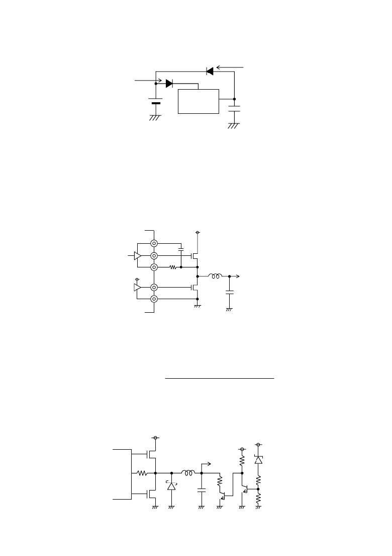
�12� )� The� SW� pin�
�When� the� SW� pin� is� connected� in� an� application,� its� coil� counter-electromotive� force� may� give� rise� to� a� single� electric�
�potential.� When� setting� up� the� application,� make� sure� that� the� SW� pin� never� exceeds� the� absolute� maximum� value.�
�Connecting� a� resistor� of� several� Ω� will� reduce� the� electric� potential.� (See� Fig.� 43)�
�Vcc�
�BOOT�
�OUTH�
�SW�
�R�
�Vo�
�Fig-42�
�OUTL�
�DGND�
�13� )� Dropout� operation�
�When� input� voltage� falls� below� approximately� output� voltage� /� 0.9� (varying� depending� on� operating� frequency)� the� ON�
�interval� on� the� OUTL� side� MOS� is� lost,� making� boost� applications� and� wrap� operation� impossible.� If� a� small� differential�
�between� input� and� output� voltage� is� envisioned� for� a� prospective� application,� connect� the� load� such� that� the� SW� voltage�
�drops� to� the� GND� level.� Managing� this� load� requires� discharging� the� SW� line� capacitance� (SW� pin� capacitance:� approx.�
�500pF;� OUTL� side� MOS� D-S� capacitance;� Schottky� capacitance).� Supported� loads� can� be� calculated� using� the� equation�
�below.�
�Output� voltage� � SW� line� capacitance�
�ILOAD� =�
�25n�
�Note� that� SW� line� capacitance� is� lower� with� smaller� loads,� and� more� stable� operation� is� attained� when� low� voltage� bias�
�circuits� are� configured� as� in� the� example� below� (Fig.� 44).� However,� the� degree� to� which� line� capacitance� is� reduced� or�
�operational� stability� is� attained� will� vary� depending� on� the� board� layout� and� components.� Therefore,� be� certain� to� confirm�
�the� effectiveness� of� these� design� factors� in� actual� operation� before� entering� mass� production.�
�Vcc�
�VREG�
�Vcc�
�OUT�
�Vo�
�SW�
�OUT�
�Fig-43�
�15/29�
�相关PDF资料 |
PDF描述 |
|---|---|
| HBC36DRTH-S13 | CONN EDGECARD 72POS .100 EXTEND |
| RBB60DHFD | CONN EDGECARD 120POS .050 SMD |
| LTC3803ES6#TRMPBF | IC REG CTRLR FLYBK PWM TSOT23-6 |
| RSC35DRXS | CONN EDGECARD 70POS DIP .100 SLD |
| HBC30DRYN | CONN EDGECARD 60POS DIP .100 SLD |
相关代理商/技术参数 |
参数描述 |
|---|---|
| BD9011KV | 制造商:ROHM 制造商全称:Rohm 功能描述:Dual Synchronous DC/DC converter controller |
| BD9011KV-E2 | 功能描述:DC/DC 开关控制器 Step Down; 2 Outputs RoHS:否 制造商:Texas Instruments 输入电压:6 V to 100 V 开关频率: 输出电压:1.215 V to 80 V 输出电流:3.5 A 输出端数量:1 最大工作温度:+ 125 C 安装风格: 封装 / 箱体:CPAK |
| BD9012KV | 制造商:ROHM 制造商全称:Rohm 功能描述:Dual-output, high voltage, high-efficiency step-down switching controller |
| BD9012KV-E2 | 功能描述:开关变换器、稳压器与控制器 Step Down; 2 Outputs RoHS:否 制造商:Texas Instruments 输出电压:1.2 V to 10 V 输出电流:300 mA 输出功率: 输入电压:3 V to 17 V 开关频率:1 MHz 工作温度范围: 安装风格:SMD/SMT 封装 / 箱体:WSON-8 封装:Reel |
| BD9013KV-E2 | 功能描述:DC/DC 开关控制器 Step Down; 2 Outputs RoHS:否 制造商:Texas Instruments 输入电压:6 V to 100 V 开关频率: 输出电压:1.215 V to 80 V 输出电流:3.5 A 输出端数量:1 最大工作温度:+ 125 C 安装风格: 封装 / 箱体:CPAK |
发布紧急采购,3分钟左右您将得到回复。