参数资料
| 型号: | BD9011EKN-E2 |
| 厂商: | Rohm Semiconductor |
| 文件页数: | 5/30页 |
| 文件大小: | 0K |
| 描述: | IC REG CTRLR BST PWM 36-HQFN |
| 标准包装: | 1 |
| PWM 型: | 控制器 |
| 输出数: | 2 |
| 频率 - 最大: | 550kHz |
| 电源电压: | 3.9 V ~ 30 V |
| 降压: | 是 |
| 升压: | 是 |
| 回扫: | 无 |
| 反相: | 无 |
| 倍增器: | 无 |
| 除法器: | 无 |
| Cuk: | 无 |
| 隔离: | 无 |
| 工作温度: | -40°C ~ 105°C |
| 封装/外壳: | 36-TQFN 裸露焊盘 |
| 包装: | 标准包装 |
| 产品目录页面: | 1372 (CN2011-ZH PDF) |
| 其它名称: | BD9011EKN-E2DKR |
第1页第2页第3页第4页当前第5页第6页第7页第8页第9页第10页第11页第12页第13页第14页第15页第16页第17页第18页第19页第20页第21页第22页第23页第24页第25页第26页第27页第28页第29页第30页
�� �
�
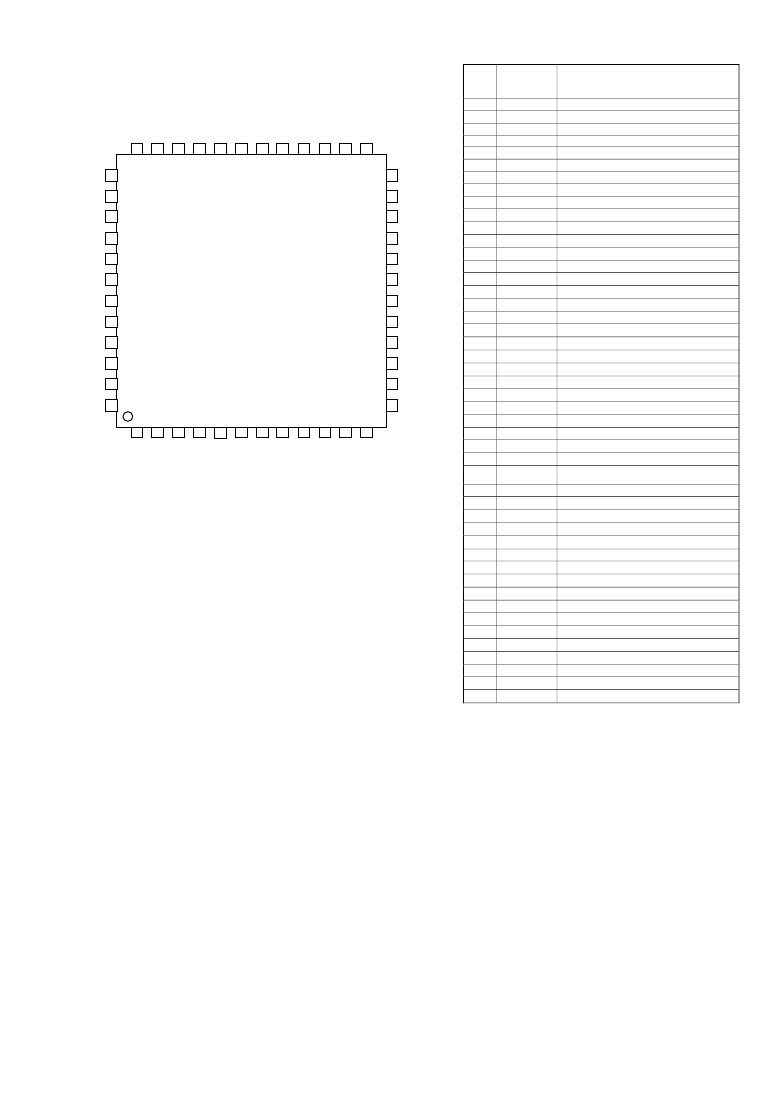
�●� Pin� configuration�
�●� Pin� function� table�
�BD9011KV� (� VQFP48C� )�
�Pin�
�No.�
�1�
�2�
�3�
�4�
�Pin� name�
�OUTH2�
�BOOT2�
�CL2�
�N.C�
�Function�
�High� side� FET� gate� drive� pin� 2�
�OUTH2� driver� power� pin�
�Over� current� detection� pin� 2�
�Non-connect� (unused)� pin�
�36�
�35�
�34�
�33�
�32�
�31�
�30�
�29�
�28�
�27�
�26�
�25�
�5�
�6�
�VCCCL2�
�N.C�
�Over� current� detection� VCC2�
�Non-connect� (unused)� pin�
�7�
�VCC�
�Input� power� pin�
�SS2� 37�
�COMP2� 38�
�FB2� 39�
�N.C� 40�
�EXTVCC� 41�
�N.C� 42�
�N.C� 43�
�VREG5� 44�
�N.C� 45�
�OUTL2� 46�
�DGND2� 47�
�SW2� 48�
�24� DET1�
�23� SS1�
�22� COMP1�
�21� FB1�
�20� N.C�
�19� VREG33�
�18� N.C�
�17� VREG5A�
�16� N.C�
�15� OUTL1�
�14� DGND1�
�13� SW1�
�8�
�9�
�10�
�11�
�12�
�13�
�14�
�15�
�16�
�17�
�18�
�19�
�20�
�21�
�22�
�23�
�24�
�25�
�26�
�27�
�VCCCL1�
�N.C�
�CL1�
�BOOT1�
�OUTH1�
�SW1�
�DGND1�
�OUTL1�
�N.C�
�VREG5A�
�N.C�
�VREG33�
�N.C�
�FB1�
�COMP1�
�SS1�
�DET1�
�STB�
�EN1�
�EN2�
�Over� current� detection� CC1�
�Non-connect� (unused)� pin�
�Over� current� detection� setting� pin� 1�
�OUTH1� driver� power� pin�
�High� side� FET� gate� drive� pin� 1�
�High� side� FET� source� pin� 1�
�Low� side� FET� source� pin� 1�
�Low� side� FET� gate� drive� pin� 1�
�Non-connect� (unused)� pin�
�FET� drive� REG� input�
�Non-connect� (unused)� pin�
�Reference� input� REG� output�
�Non-connect� (unused)� pin�
�Error� amp� input� 1�
�Error� amp� output� 1�
�Soft� start� setting� pin� 1�
�FB� detector� output� 1�
�Standby� ON/OFF� pin�
�Output� 1� ON/OFF� pin�
�Output� 2� ON/OFF� pin�
�1�
�2�
�3�
�4�
�5�
�6�
�7�
�8�
�9�
�10�
�11�
�12�
�28�
�N.C�
�Non-connect� (unused)� pin�
�29�
�30�
�31�
�32�
�GND�
�GNDS�
�LOFF�
�N.C�
�Ground�
�Sense� ground�
�Over� current� protection� OFF� latch�
�function� ON/OFF� pin�
�Non-connect� (unused)� pin�
�Fig-15�
�33�
�34�
�35�
�36�
�37�
�38�
�39�
�40�
�41�
�42�
�43�
�44�
�45�
�46�
�47�
�48�
�RT�
�SYNC�
�LLM�
�DET2�
�SS2�
�COMP2�
�FB2�
�N.C�
�EXTVCC�
�N.C�
�N.C�
�VREG5�
�N.C�
�OUTL2�
�DGND2�
�SW2�
�Switching� frequency� setting� pin�
�External� synchronous� pulse� input� pin�
�Built-in� pull-down� resistor� pin�
�FB� detector� output� 2�
�Soft� start� setting� pin� 2�
�Error� amp� output� 2�
�Error� amp� input� 2�
�Non-connect� (unused)� pin�
�External� power� input� pin�
�Non-connect� (unused)� pin�
�Non-connect� (unused)� pin�
�FET� drive� REG� output�
�Non-connect� (unused)� pin�
�Low� side� FET� gate� drive� pin� 2�
�Low� side� FET� source� pin� 2�
�High� side� FET� source� pin� 2�
�●� Block� functional� descriptions�
�?� Error� amp�
�The� error� amp� compares� output� feedback� voltage� to� the� 0.8V� reference� voltage� and� provides� the� comparison� result� as� COMP� voltage,� which� is�
�used� to� determine� the� switching� Duty.� COMP� voltage� is� limited� to� the� SS� voltage,� since� soft� start� at� power� up� is� based� on� SS� pin� voltage.�
�?� Oscillator� (OSC)�
�Oscillation� frequency� is� determined� by� the� switching� frequency� pin� (RT)� in� this� block.� The� frequency� can� be� set� between� 250kHz� and� 550kHz.�
�?� SLOPE�
�The� SLOPE� block� uses� the� clock� produced� by� the� oscillator� to� generate� a� triangular� wave,� and� sends� the� wave� to� the� PWM� comparator.�
�?� PWM� COMP�
�The� PWM� comparator� determines� switching� Duty� by� comparing� the� COMP� voltage,� output� from� the� error� amp,� with� the� triangular� wave� from� the�
�SLOPE� block.� Switching� duty� is� limited� to� a� percentage� of� the� internal� maximum� duty,� and� thus� cannot� be� 100%� of� the� maximum.�
�?� Reference� voltage� (5Vreg� ,� 33Vreg)�
�This� block� generates� the� internal� reference� voltages:� 5V� and� 3.3V.�
�?� External� synchronization� (SYNC)�
�Determines� the� switching� frequency,� based� on� the� external� pulse� applied.�
�?� Over� current� protection� (OCP)�
�Over� current� protection� is� activated� when� the� VCCCL-CL� voltage� reaches� or� exceeds� 90mV.� When� over� current� protection� is� active,� Duty� is� low,�
�and� output� voltage� also� decreases.� When� LOFF=L,� the� output� voltage� has� fallen� to� 70%� or� below� and� output� is� latched� OFF.� The� OFF� latch�
�mode� ends� when� the� latch� is� set� to� STB,� EN.�
�?� Sequence� control� (Sequence� DET)�
�Compares� FB� voltage� with� reference� voltage� (0.56V)� and� outputs� the� result� as� DET.�
�?� Protection� circuits� (UVLO/TSD)�
�The� UVLO� lock� out� function� is� activated� when� VREG� falls� to� about� 2.8V,� while� TSD� turns� outputs� OFF� when� the� chip� temperature� reaches� or�
�exceeds� 150� ℃� .� Output� is� restored� when� temperature� falls� back� below� the� threshold� value.�
�5/29�
�相关PDF资料 |
PDF描述 |
|---|---|
| HBC36DRTH-S13 | CONN EDGECARD 72POS .100 EXTEND |
| RBB60DHFD | CONN EDGECARD 120POS .050 SMD |
| LTC3803ES6#TRMPBF | IC REG CTRLR FLYBK PWM TSOT23-6 |
| RSC35DRXS | CONN EDGECARD 70POS DIP .100 SLD |
| HBC30DRYN | CONN EDGECARD 60POS DIP .100 SLD |
相关代理商/技术参数 |
参数描述 |
|---|---|
| BD9011KV | 制造商:ROHM 制造商全称:Rohm 功能描述:Dual Synchronous DC/DC converter controller |
| BD9011KV-E2 | 功能描述:DC/DC 开关控制器 Step Down; 2 Outputs RoHS:否 制造商:Texas Instruments 输入电压:6 V to 100 V 开关频率: 输出电压:1.215 V to 80 V 输出电流:3.5 A 输出端数量:1 最大工作温度:+ 125 C 安装风格: 封装 / 箱体:CPAK |
| BD9012KV | 制造商:ROHM 制造商全称:Rohm 功能描述:Dual-output, high voltage, high-efficiency step-down switching controller |
| BD9012KV-E2 | 功能描述:开关变换器、稳压器与控制器 Step Down; 2 Outputs RoHS:否 制造商:Texas Instruments 输出电压:1.2 V to 10 V 输出电流:300 mA 输出功率: 输入电压:3 V to 17 V 开关频率:1 MHz 工作温度范围: 安装风格:SMD/SMT 封装 / 箱体:WSON-8 封装:Reel |
| BD9013KV-E2 | 功能描述:DC/DC 开关控制器 Step Down; 2 Outputs RoHS:否 制造商:Texas Instruments 输入电压:6 V to 100 V 开关频率: 输出电压:1.215 V to 80 V 输出电流:3.5 A 输出端数量:1 最大工作温度:+ 125 C 安装风格: 封装 / 箱体:CPAK |
发布紧急采购,3分钟左右您将得到回复。