- 您现在的位置:买卖IC网 > Datasheet目录398 > BSS84_D87Z (Fairchild Semiconductor)MOSFET P-CH 50V 130MA SOT-23 Datasheet资料下载
参数资料
| 型号: | BSS84_D87Z |
| 厂商: | Fairchild Semiconductor |
| 文件页数: | 1/6页 |
| 文件大小: | 0K |
| 描述: | MOSFET P-CH 50V 130MA SOT-23 |
| 标准包装: | 10,000 |
| FET 型: | MOSFET P 通道,金属氧化物 |
| FET 特点: | 逻辑电平门 |
| 漏极至源极电压(Vdss): | 50V |
| 电流 - 连续漏极(Id) @ 25° C: | 130mA |
| 开态Rds(最大)@ Id, Vgs @ 25° C: | 10 欧姆 @ 100mA,5V |
| Id 时的 Vgs(th)(最大): | 2V @ 1mA |
| 闸电荷(Qg) @ Vgs: | 1.3nC @ 5V |
| 输入电容 (Ciss) @ Vds: | 73pF @ 25V |
| 功率 - 最大: | 360mW |
| 安装类型: | 表面贴装 |
| 封装/外壳: | TO-236-3,SC-59,SOT-23-3 |
| 供应商设备封装: | SOT-23 |
| 包装: | 带卷 (TR) |
�� �
�
�February� 2013�
�BSS84�
�P-Channel� Enhancement� Mode� Field-Effect� Transistor�
�Features�
�Description�
�?�
�?�
�?�
�?�
�-0.13� A,� -50� V,� R� DS(ON)� =� 10� Ω� at� V� GS� =� -5� V�
�Voltage-Controlled� P-Channel� Small-Signal�
�Switch�
�High-Density� Cell� Design� for� Low� R� DS(ON)�
�High� Saturation� Current�
�This� P-channel� enhancement-mode� field-effect�
�transistor� is� produced� using� Fairchild’s� proprietary,�
�high� cell� density,� DMOS� technology.� This� very� high�
�density� process� minimizes� on-state� resistance� and� to�
�provide� rugged� and� reliable� performance� and� fast�
�switching.� The� BSS84� can� be� used,� with� a� minimum�
�of� effort,� in� most� applications� requiring� up� to� 0.13� A�
�D�
�D�
�DC� and� can� deliver� current� up� to� 0.52� A.� This� product�
�is� particularly� suited� to� low-voltage� applications�
�requiring� a� low-current� high-side� switch.�
�S�
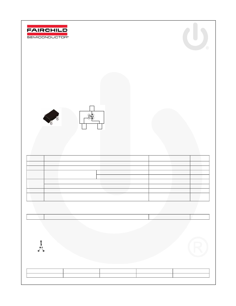
�SOT-23�
�G�
�G�
�S�
�Absolute� Maximum� Ratings�
�Stresses� exceeding� the� absolute� maximum� ratings� may� damage� the� device.� The� device� may� not� function� or� be�
�operable� above� the� recommended� operating� conditions� and� stressing� the� parts� to� these� levels� is� not� recommended.�
�In� addition,� extended� exposure� to� stresses� above� the� recommended� operating� conditions� may� affect� device� reliability.�
�The� absolute� maximum� ratings� are� stress� ratings� only.� Values� are� at� T� A� =� 25°C� unless� otherwise� noted.�
�Drain� Current� (1)�
�Symbol�
�V� DSS�
�V� GSS�
�I� D�
�P� D�
�T� J� ,� T� STG�
�T� L�
�Parameter�
�Drain-Source� Voltage�
�Gate-Source� Voltage�
�Continuous�
�Pulsed�
�Maximum� Power� Dissipation� (1)�
�Derate� Above� 25� °� C�
�Operating� and� Storage� Junction� Temperature� Range�
�Maximum� Lead� Temperature� for� Soldering�
�Purposes,� 1/16”� from� Case� for� 10� Seconds�
�Ratings�
�?� 50�
�±� 20�
�?� 0.13�
�?� 0.52�
�0.36�
�2.9�
�?� 55� to� +150�
�300�
�Unit�
�V�
�V�
�A�
�A�
�W�
�mW� /� °� C�
�°� C�
�°� C�
�Thermal� Characteristics�
�R� θ� JA�
�Thermal� Resistance,� Junction-to-Ambient� (1)�
�350�
�°� C/W�
�Note:�
�1.� R� θ� JA� is� the� sum� of� the� junction-to-case� and� case-to-ambient� thermal� resistance� where� the� case� thermal� reference�
�is� defined� as� the� solder� mounting� surface� of� the� drain� pins.� R� θ� JA� is� guaranteed� by� design,� while� R� θ� JA� is�
�determined� by� the� user's� board� design.�
�a)� 350°C/W� when� mounted� on� a� minimum� pad�
�Scale� 1:� 1� on� letter-size� paper.�
�Package� Marking� and� Ordering� Information�
�Device� Marking�
�SP�
�Device�
�BSS84�
�Reel� Size�
�7’’�
�Tape� width�
�8mm�
�Quantity�
�3000�
�?� 2002� Fairchild� Semiconductor� Corporation�
�BSS84� ?� Rev.� 1.1.0�
�www.fairchildsemi.com�
�相关PDF资料 |
PDF描述 |
|---|---|
| BSS8402DW-7 | MOSFET N+P 50,60V 130MA SC70-6 |
| BSS84DW-7 | MOSFET DUAL P-CHAN -50V SC70-6 |
| BSS84LT1 | MOSFET P-CH 50V 130MA SOT-23 |
| BSS84TC | MOSFET P-CHAN 50V SOT23-3 |
| BSS84V-7 | MOSFET P-CH DUAL SOT-563 |
相关代理商/技术参数 |
参数描述 |
|---|---|
| BSS84DW | 制造商:DIODES 制造商全称:Diodes Incorporated 功能描述:DUAL P-CHANNEL ENHANCEMENT MODE FIELD EFFECT TRANSISTOR |
| BSS84DW _R1 _00001 | 制造商:PanJit Touch Screens 功能描述: |
| BSS84DW_ R2 _00001 | 制造商:PanJit Touch Screens 功能描述: |
| BSS84DW_1 | 制造商:DIODES 制造商全称:Diodes Incorporated 功能描述:DUAL P-CHANNEL ENHANCEMENT MODE FIELD EFFECT TRANSISTOR |
| BSS84DW_2 | 制造商:DIODES 制造商全称:Diodes Incorporated 功能描述:DUAL P-CHANNEL ENHANCEMENT MODE FIELD EFFECT TRANSISTOR |
发布紧急采购,3分钟左右您将得到回复。