- 您现在的位置:买卖IC网 > PDF目录15868 > C8051F000-TB (Silicon Laboratories Inc)BOARD PROTOTYPING W/C8051F000 PDF资料下载
参数资料
| 型号: | C8051F000-TB |
| 厂商: | Silicon Laboratories Inc |
| 文件页数: | 28/171页 |
| 文件大小: | 0K |
| 描述: | BOARD PROTOTYPING W/C8051F000 |
| 标准包装: | 1 |
第1页第2页第3页第4页第5页第6页第7页第8页第9页第10页第11页第12页第13页第14页第15页第16页第17页第18页第19页第20页第21页第22页第23页第24页第25页第26页第27页当前第28页第29页第30页第31页第32页第33页第34页第35页第36页第37页第38页第39页第40页第41页第42页第43页第44页第45页第46页第47页第48页第49页第50页第51页第52页第53页第54页第55页第56页第57页第58页第59页第60页第61页第62页第63页第64页第65页第66页第67页第68页第69页第70页第71页第72页第73页第74页第75页第76页第77页第78页第79页第80页第81页第82页第83页第84页第85页第86页第87页第88页第89页第90页第91页第92页第93页第94页第95页第96页第97页第98页第99页第100页第101页第102页第103页第104页第105页第106页第107页第108页第109页第110页第111页第112页第113页第114页第115页第116页第117页第118页第119页第120页第121页第122页第123页第124页第125页第126页第127页第128页第129页第130页第131页第132页第133页第134页第135页第136页第137页第138页第139页第140页第141页第142页第143页第144页第145页第146页第147页第148页第149页第150页第151页第152页第153页第154页第155页第156页第157页第158页第159页第160页第161页第162页第163页第164页第165页第166页第167页第168页第169页第170页第171页
C8051F000/1/2/5/6/7
C8051F010/1/2/5/6/7
17. SERIAL PERIPHERAL INTERFACE BUS
The Serial Peripheral Interface (SPI) provides access to a four-wire, full-duplex, serial bus. SPI supports the
connection of multiple slave devices to a master device on the same bus. A separate slave-select signal (NSS) is
used to select a slave device and enable a data transfer between the master and the selected slave. Multiple masters
on the same bus are also supported. Collision detection is provided when two or more masters attempt a data
transfer at the same time. The SPI can operate as either a master or a slave. When the SPI is configured as a
master, the maximum data transfer rate (bits/sec) is one-half the system clock frequency.
When the SPI is configured as a slave, the maximum data transfer rate (bits/sec) for full-duplex operation is 1/10 the
system clock frequency, provided that the master issues SCK, NSS, and the serial input data synchronously with the
system clock. If the master issues SCK, NSS, and the serial input data asynchronously, the maximum data transfer
rate (bits/sec) must be less that 1/10 the system clock frequency. In the special case where the master only wants to
transmit data to the slave and does not need to receive data from the slave (i.e. half-duplex operation), the SPI slave
can receive data at a maximum data transfer rate (bits/sec) of the system clock frequency. This is provided that
the master issues SCK, NSS, and the serial input data synchronously with the system clock.
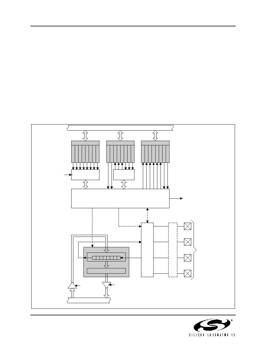
Figure 17.1. SPI Block Diagram
SFR Bus
Clock Divide
Logic
Data Path
Control
SFR Bus
Write to
SPI0DAT
Receive Data Register
SPI0DAT
0
1
2
3
4
5
6
7
Shift Register
SPI CONTROL LOGIC
Bit Count
Logic
SPI0CKR
S
C
R
7
S
C
R
6
S
C
R
5
S
C
R
4
S
C
R
3
S
C
R
2
S
C
R
1
S
C
R
0
SPI0CFG
C
K
P
H
A
C
K
P
O
L
B
C
2
B
C
1
B
C
0
F
R
S
2
F
R
S
1
F
R
S
0
SPI0CN
M
O
D
F
T
X
B
S
Y
S
L
V
S
E
L
M
S
T
E
N
S
P
I
E
N
W
C
O
L
S
P
I
F
R
X
O
V
R
N
Pin Control
Interface
SPI Clock
(Master Mode)
Pin
Control
Logic
C
R
O
S
B
A
R
Port I/O
Read
SPI0DAT
SPI IRQ
SYSCLK
Tx Data
Rx Data
SCK
MOSI
MISO
NSS
123
Rev. 1.7
相关PDF资料 |
PDF描述 |
|---|---|
| RP15-4812DF/N-HC | CONV DC/DC 15W 36-75VIN +/-12V |
| MAX6439UTAHTD3+T | IC BATTERY MON SNGL SOT23-6 |
| C8051F124-TB | BOARD PROTOTYPING W/C8051F124 |
| SDR1105-560KL | INDUCTOR 56UH 2A SMD |
| GBM22DREH | CONN EDGECARD 44POS .156 EYELET |
相关代理商/技术参数 |
参数描述 |
|---|---|
| C8051F001 | 功能描述:8位微控制器 -MCU 32KB 12ADC RoHS:否 制造商:Silicon Labs 核心:8051 处理器系列:C8051F39x 数据总线宽度:8 bit 最大时钟频率:50 MHz 程序存储器大小:16 KB 数据 RAM 大小:1 KB 片上 ADC:Yes 工作电源电压:1.8 V to 3.6 V 工作温度范围:- 40 C to + 105 C 封装 / 箱体:QFN-20 安装风格:SMD/SMT |
| C8051F001-GQ | 功能描述:8位微控制器 -MCU 32KB 12ADC RoHS:否 制造商:Silicon Labs 核心:8051 处理器系列:C8051F39x 数据总线宽度:8 bit 最大时钟频率:50 MHz 程序存储器大小:16 KB 数据 RAM 大小:1 KB 片上 ADC:Yes 工作电源电压:1.8 V to 3.6 V 工作温度范围:- 40 C to + 105 C 封装 / 箱体:QFN-20 安装风格:SMD/SMT |
| C8051F001-GQR | 功能描述:8位微控制器 -MCU 32KB 12ADC 48Pin MCU Tape and Reel RoHS:否 制造商:Silicon Labs 核心:8051 处理器系列:C8051F39x 数据总线宽度:8 bit 最大时钟频率:50 MHz 程序存储器大小:16 KB 数据 RAM 大小:1 KB 片上 ADC:Yes 工作电源电压:1.8 V to 3.6 V 工作温度范围:- 40 C to + 105 C 封装 / 箱体:QFN-20 安装风格:SMD/SMT |
| C8051F001R | 功能描述:8位微控制器 -MCU C 12Bit 48Pin RoHS:否 制造商:Silicon Labs 核心:8051 处理器系列:C8051F39x 数据总线宽度:8 bit 最大时钟频率:50 MHz 程序存储器大小:16 KB 数据 RAM 大小:1 KB 片上 ADC:Yes 工作电源电压:1.8 V to 3.6 V 工作温度范围:- 40 C to + 105 C 封装 / 箱体:QFN-20 安装风格:SMD/SMT |
| C8051F002 | 功能描述:8位微控制器 -MCU 32KB 12ADC RoHS:否 制造商:Silicon Labs 核心:8051 处理器系列:C8051F39x 数据总线宽度:8 bit 最大时钟频率:50 MHz 程序存储器大小:16 KB 数据 RAM 大小:1 KB 片上 ADC:Yes 工作电源电压:1.8 V to 3.6 V 工作温度范围:- 40 C to + 105 C 封装 / 箱体:QFN-20 安装风格:SMD/SMT |
发布紧急采购,3分钟左右您将得到回复。