- 您现在的位置:买卖IC网 > PDF目录3798 > C8051F236-GQ (Silicon Laboratories Inc)IC 8051 MCU 8K FLASH 48TQFP PDF资料下载
参数资料
| 型号: | C8051F236-GQ |
| 厂商: | Silicon Laboratories Inc |
| 文件页数: | 48/146页 |
| 文件大小: | 0K |
| 描述: | IC 8051 MCU 8K FLASH 48TQFP |
| 产品培训模块: | Serial Communication Overview |
| 标准包装: | 250 |
| 系列: | C8051F2xx |
| 核心处理器: | 8051 |
| 芯体尺寸: | 8-位 |
| 速度: | 25MHz |
| 连通性: | SPI,UART/USART |
| 外围设备: | 欠压检测/复位,POR,WDT |
| 输入/输出数: | 32 |
| 程序存储器容量: | 8KB(8K x 8) |
| 程序存储器类型: | 闪存 |
| RAM 容量: | 1.25K x 8 |
| 电压 - 电源 (Vcc/Vdd): | 2.7 V ~ 3.6 V |
| 振荡器型: | 内部 |
| 工作温度: | -40°C ~ 85°C |
| 封装/外壳: | 48-TQFP |
| 包装: | 托盘 |
| 产品目录页面: | 623 (CN2011-ZH PDF) |
| 其它名称: | 336-1244 |
第1页第2页第3页第4页第5页第6页第7页第8页第9页第10页第11页第12页第13页第14页第15页第16页第17页第18页第19页第20页第21页第22页第23页第24页第25页第26页第27页第28页第29页第30页第31页第32页第33页第34页第35页第36页第37页第38页第39页第40页第41页第42页第43页第44页第45页第46页第47页当前第48页第49页第50页第51页第52页第53页第54页第55页第56页第57页第58页第59页第60页第61页第62页第63页第64页第65页第66页第67页第68页第69页第70页第71页第72页第73页第74页第75页第76页第77页第78页第79页第80页第81页第82页第83页第84页第85页第86页第87页第88页第89页第90页第91页第92页第93页第94页第95页第96页第97页第98页第99页第100页第101页第102页第103页第104页第105页第106页第107页第108页第109页第110页第111页第112页第113页第114页第115页第116页第117页第118页第119页第120页第121页第122页第123页第124页第125页第126页第127页第128页第129页第130页第131页第132页第133页第134页第135页第136页第137页第138页第139页第140页第141页第142页第143页第144页第145页第146页
C8051F2xx
Rev. 1.6
141
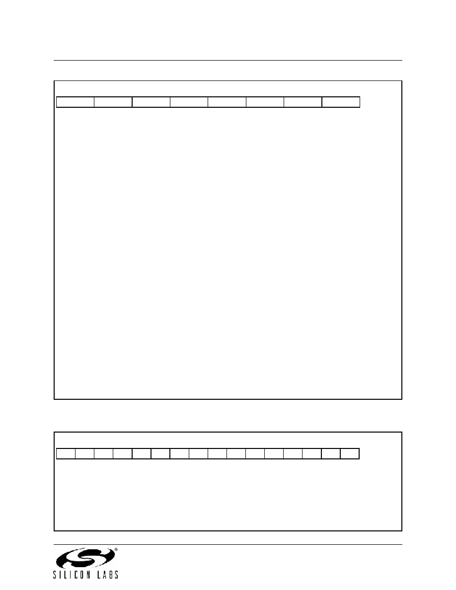
JTAG Register Definition 18.2. FLASHCON: JTAG Flash Control
This register determines how the Flash interface logic will respond to reads and writes to the FLASH-
DAT Register.
Bits7–4: WRMD3–0: Write Mode Select Bits.
The Write Mode Select Bits control how the interface logic responds to writes to the FLASH-
DAT Register per the following values:
0000:
A FLASHDAT write replaces the data in the FLASHDAT register, but is otherwise
ignored.
0001:
A FLASHDAT write initiates a write of FLASHDAT into the memory address selected
by the FLASHADR register. FLASHADR is incremented by one when complete.
0010:
A FLASHDAT write initiates an erasure (sets all bytes to 0xFF) of the Flash page
containing the address in FLASHADR. FLASHDAT must be 0xA5 for the erase to
occur. FLASHADR is not affected. If FLASHADR = 0x1DFE – 0x1DFF, the entire
user space will be erased (i.e. entire Flash memory except for Reserved area
0x1E00 – 0x1FFF).
(All other values for WRMD3–0 are reserved.)
Bits3–0: RDMD3–0: Read Mode Select Bits.
The Read Mode Select Bits control how the interface logic responds to reads to the FLASH-
DAT Register per the following values:
0000:
A FLASHDAT read provides the data in the FLASHDAT register, but is otherwise
ignored.
0001:
A FLASHDAT read initiates a read of the byte addressed by the FLASHADR register
if no operation is currently active. This mode is used for block reads.
0010:
A FLASHDAT read initiates a read of the byte addressed by FLASHADR only if no
operation is active and any data from a previous read has already been read from
FLASHDAT. This mode allows single bytes to be read (or the last byte of a block)
without initiating an extra read.
(All other values for RDMD3–0 are reserved.)
JTAG Register Definition 18.3. FLASHADR: JTAG Flash Address
This register holds the address for all JTAG Flash read, write, and erase operations. This register
autoincrements after each read or write, regardless of whether the operation succeeded or failed.
Bits15–0: Flash Operation 16-bit Address.
Reset Value
WRMD3
WRMD2
WRMD1
WRMD0
RDMD3
RDMD2
RDMD1
RDMD0
00000000
Bit7
Bit6
Bit5
Bit4
Bit3
Bit2
Bit1
Bit0
Reset Value
0x0000
Bit15
Bit0
相关PDF资料 |
PDF描述 |
|---|---|
| USB-B-S-F-B-SM-R-TR | USB TYPE B 2.0 BLACK SMD |
| USB-A-S-F-W-SM2-R-TR | USB TYPE A WHITE SNGL SMD |
| USB-B-S-F-W-TH | USB TYPE B 2.0 WHITE T/H |
| P87C52X2BN,112 | IC 80C51 MCU 8K OTP 40-DIP |
| USB-B-S-F-B-TH-R | USB TYPE B 2.0 BLACK T/H |
相关代理商/技术参数 |
参数描述 |
|---|---|
| C8051F236-GQR | 功能描述:8位微控制器 -MCU 8KB 1KRam 48Pin MCU Tape and Reel RoHS:否 制造商:Silicon Labs 核心:8051 处理器系列:C8051F39x 数据总线宽度:8 bit 最大时钟频率:50 MHz 程序存储器大小:16 KB 数据 RAM 大小:1 KB 片上 ADC:Yes 工作电源电压:1.8 V to 3.6 V 工作温度范围:- 40 C to + 105 C 封装 / 箱体:QFN-20 安装风格:SMD/SMT |
| C8051F236R | 功能描述:8位微控制器 -MCU T-01280 Ram 48Pin RoHS:否 制造商:Silicon Labs 核心:8051 处理器系列:C8051F39x 数据总线宽度:8 bit 最大时钟频率:50 MHz 程序存储器大小:16 KB 数据 RAM 大小:1 KB 片上 ADC:Yes 工作电源电压:1.8 V to 3.6 V 工作温度范围:- 40 C to + 105 C 封装 / 箱体:QFN-20 安装风格:SMD/SMT |
| C8051F2XX | 制造商:未知厂家 制造商全称:未知厂家 功能描述:Mixed Signal 8 kB ISP Flash MCU Family |
| C8051F300 | 功能描述:8位微控制器 -MCU 8KB 8ADC 2%osc RoHS:否 制造商:Silicon Labs 核心:8051 处理器系列:C8051F39x 数据总线宽度:8 bit 最大时钟频率:50 MHz 程序存储器大小:16 KB 数据 RAM 大小:1 KB 片上 ADC:Yes 工作电源电压:1.8 V to 3.6 V 工作温度范围:- 40 C to + 105 C 封装 / 箱体:QFN-20 安装风格:SMD/SMT |
| C8051F300DK | 功能描述:开发板和工具包 - 8051 MCU DEVELOPMENT KIT W/ US POWER SUPPLY RoHS:否 制造商:Silicon Labs 产品:Development Kits 工具用于评估:C8051F960, Si7005 核心: 接口类型:USB 工作电源电压: |
发布紧急采购,3分钟左右您将得到回复。