- 您现在的位置:买卖IC网 > PDF目录3798 > C8051F236-GQ (Silicon Laboratories Inc)IC 8051 MCU 8K FLASH 48TQFP PDF资料下载
参数资料
| 型号: | C8051F236-GQ |
| 厂商: | Silicon Laboratories Inc |
| 文件页数: | 65/146页 |
| 文件大小: | 0K |
| 描述: | IC 8051 MCU 8K FLASH 48TQFP |
| 产品培训模块: | Serial Communication Overview |
| 标准包装: | 250 |
| 系列: | C8051F2xx |
| 核心处理器: | 8051 |
| 芯体尺寸: | 8-位 |
| 速度: | 25MHz |
| 连通性: | SPI,UART/USART |
| 外围设备: | 欠压检测/复位,POR,WDT |
| 输入/输出数: | 32 |
| 程序存储器容量: | 8KB(8K x 8) |
| 程序存储器类型: | 闪存 |
| RAM 容量: | 1.25K x 8 |
| 电压 - 电源 (Vcc/Vdd): | 2.7 V ~ 3.6 V |
| 振荡器型: | 内部 |
| 工作温度: | -40°C ~ 85°C |
| 封装/外壳: | 48-TQFP |
| 包装: | 托盘 |
| 产品目录页面: | 623 (CN2011-ZH PDF) |
| 其它名称: | 336-1244 |
第1页第2页第3页第4页第5页第6页第7页第8页第9页第10页第11页第12页第13页第14页第15页第16页第17页第18页第19页第20页第21页第22页第23页第24页第25页第26页第27页第28页第29页第30页第31页第32页第33页第34页第35页第36页第37页第38页第39页第40页第41页第42页第43页第44页第45页第46页第47页第48页第49页第50页第51页第52页第53页第54页第55页第56页第57页第58页第59页第60页第61页第62页第63页第64页当前第65页第66页第67页第68页第69页第70页第71页第72页第73页第74页第75页第76页第77页第78页第79页第80页第81页第82页第83页第84页第85页第86页第87页第88页第89页第90页第91页第92页第93页第94页第95页第96页第97页第98页第99页第100页第101页第102页第103页第104页第105页第106页第107页第108页第109页第110页第111页第112页第113页第114页第115页第116页第117页第118页第119页第120页第121页第122页第123页第124页第125页第126页第127页第128页第129页第130页第131页第132页第133页第134页第135页第136页第137页第138页第139页第140页第141页第142页第143页第144页第145页第146页
C8051F2xx
Rev. 1.6
25
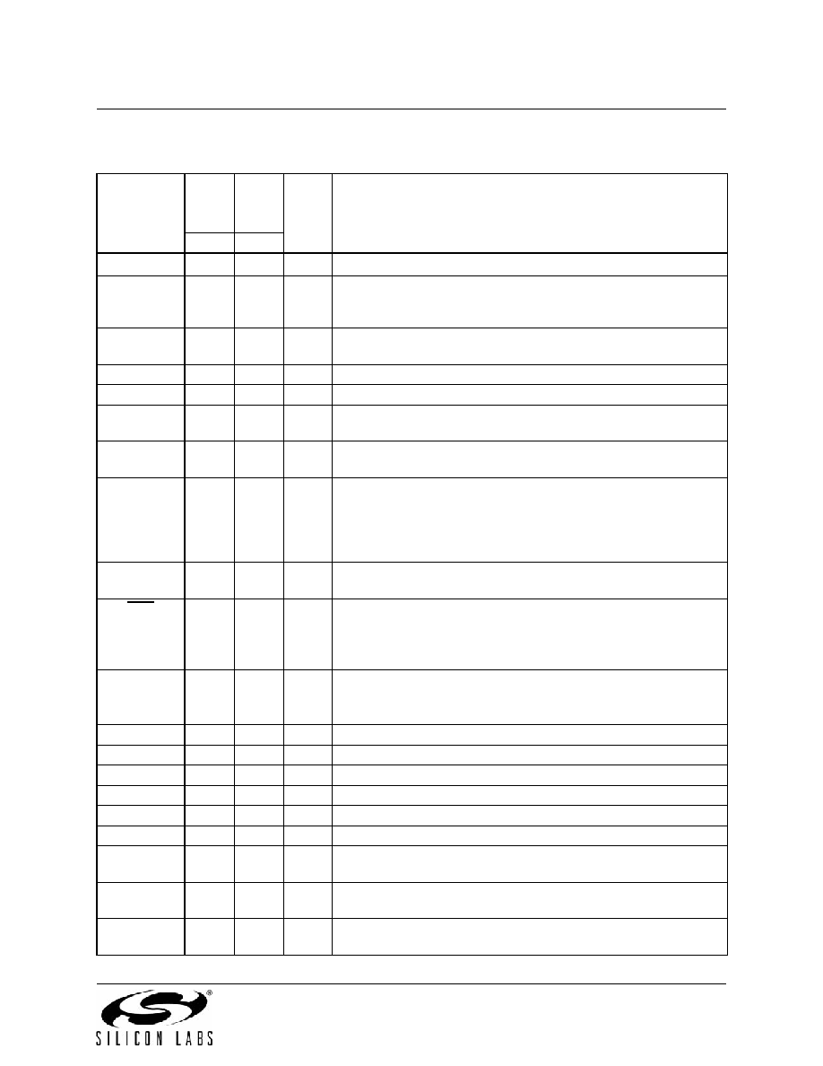
4.
Pinout and Package Definitions
Table 4.1. Pin Definitions
Name
‘F206,
F220,
226,
230,
236
‘F221,
231
Type
Description
48-Pin 32-Pin
VDD
11,31
8
Digital Voltage Supply.
GND
5,6,8,
13,32
9
Ground. (
Note: Pins 5,6, and 8 on the 48-pin package are not
connected (NC), but it is recommended that they be connected to
ground.)
MONEN
12
D In
Monitor Enable (on 48 pin package ONLY). Enables reset volt-
age monitor function when pulled high (logic “1”).
TCK
25
17
D In
JTAG Test Clock with internal pull-up.
TMS
26
18
D In
JTAG Test-Mode Select with internal pull-up.
TDI
28
20
D In
JTAG Test Data Input with internal pull-up. TDI is latched on a
rising edge of TCK.
TDO
27
19
D Out JTAG Test Data Output. Data is shifted out on TDO on the falling
edge of TCK. TDO output is a tri-state driver.
XTAL1
9
6
A In
Crystal Input. This pin is the return for the internal oscillator cir-
cuit for a crystal or ceramic resonator. For a precision internal
clock, connect a crystal or ceramic resonator from XTAL1 to
XTAL2. If overdriven by an external CMOS clock, this becomes
the system clock.
XTAL2
10
7
A Out
Crystal Output. This pin is the excitation driver for a crystal or
ceramic resonator.
RST
14
10
D I/O
Chip Reset. Open-drain output of internal Voltage Supply moni-
tor. Is driven low when VDD is < 2.7V and MONEN=1, or when a
‘1’is written to PORSF. An external source can force a system
reset by driving this pin low.
VREF
7
5
A I/O
Voltage Reference. When configured as an input, this pin is the
voltage reference for the ADC. Otherwise, VDD will be the refer-
ence. NOTE: this pin is Not Connected (NC) on ‘F230/1/6.
CP0+
4
A In
Comparator 0 Non-Inverting Input.
CP0-
3
A In
Comparator 0 Inverting Input.
CP0
2
D Out
Comparator 0 Output
CP1+
1
A In
Comparator 1 Non-Inverting Input.
CP1-
48
32
A In
Comparator 1 Inverting Input.
CP1
47
31
D Out
Comparator 1 Output
P0.0/TX
40
28
D I/O
A In
Port0 Bit0. (See the Port I/O Sub-System section for complete
description).
P0.1/RX
39
27
D I/O
A In
Port0 Bit1. (See the Port I/O Sub-System section for complete
description).
P0.2/INT0
38
26
D I/O
A In
Port0 Bit2. (See the Port I/O Sub-System section for complete
description).
相关PDF资料 |
PDF描述 |
|---|---|
| USB-B-S-F-B-SM-R-TR | USB TYPE B 2.0 BLACK SMD |
| USB-A-S-F-W-SM2-R-TR | USB TYPE A WHITE SNGL SMD |
| USB-B-S-F-W-TH | USB TYPE B 2.0 WHITE T/H |
| P87C52X2BN,112 | IC 80C51 MCU 8K OTP 40-DIP |
| USB-B-S-F-B-TH-R | USB TYPE B 2.0 BLACK T/H |
相关代理商/技术参数 |
参数描述 |
|---|---|
| C8051F236-GQR | 功能描述:8位微控制器 -MCU 8KB 1KRam 48Pin MCU Tape and Reel RoHS:否 制造商:Silicon Labs 核心:8051 处理器系列:C8051F39x 数据总线宽度:8 bit 最大时钟频率:50 MHz 程序存储器大小:16 KB 数据 RAM 大小:1 KB 片上 ADC:Yes 工作电源电压:1.8 V to 3.6 V 工作温度范围:- 40 C to + 105 C 封装 / 箱体:QFN-20 安装风格:SMD/SMT |
| C8051F236R | 功能描述:8位微控制器 -MCU T-01280 Ram 48Pin RoHS:否 制造商:Silicon Labs 核心:8051 处理器系列:C8051F39x 数据总线宽度:8 bit 最大时钟频率:50 MHz 程序存储器大小:16 KB 数据 RAM 大小:1 KB 片上 ADC:Yes 工作电源电压:1.8 V to 3.6 V 工作温度范围:- 40 C to + 105 C 封装 / 箱体:QFN-20 安装风格:SMD/SMT |
| C8051F2XX | 制造商:未知厂家 制造商全称:未知厂家 功能描述:Mixed Signal 8 kB ISP Flash MCU Family |
| C8051F300 | 功能描述:8位微控制器 -MCU 8KB 8ADC 2%osc RoHS:否 制造商:Silicon Labs 核心:8051 处理器系列:C8051F39x 数据总线宽度:8 bit 最大时钟频率:50 MHz 程序存储器大小:16 KB 数据 RAM 大小:1 KB 片上 ADC:Yes 工作电源电压:1.8 V to 3.6 V 工作温度范围:- 40 C to + 105 C 封装 / 箱体:QFN-20 安装风格:SMD/SMT |
| C8051F300DK | 功能描述:开发板和工具包 - 8051 MCU DEVELOPMENT KIT W/ US POWER SUPPLY RoHS:否 制造商:Silicon Labs 产品:Development Kits 工具用于评估:C8051F960, Si7005 核心: 接口类型:USB 工作电源电压: |
发布紧急采购,3分钟左右您将得到回复。