- 您现在的位置:买卖IC网 > Datasheet目录317 > C8051T610DB24 (Silicon Laboratories Inc)DAUGHTER BOARD T610 24QFN SOCKET Datasheet资料下载
参数资料
| 型号: | C8051T610DB24 |
| 厂商: | Silicon Laboratories Inc |
| 文件页数: | 160/218页 |
| 文件大小: | 0K |
| 描述: | DAUGHTER BOARD T610 24QFN SOCKET |
| 标准包装: | 1 |
| 模块/板类型: | QFN 插口模块 |
| 适用于相关产品: | C8051T610DK |
| 相关产品: | 336-1443-ND - KIT DEV FOR C8051T61X MCU'S |
| 其它名称: | 336-1507 |
第1页第2页第3页第4页第5页第6页第7页第8页第9页第10页第11页第12页第13页第14页第15页第16页第17页第18页第19页第20页第21页第22页第23页第24页第25页第26页第27页第28页第29页第30页第31页第32页第33页第34页第35页第36页第37页第38页第39页第40页第41页第42页第43页第44页第45页第46页第47页第48页第49页第50页第51页第52页第53页第54页第55页第56页第57页第58页第59页第60页第61页第62页第63页第64页第65页第66页第67页第68页第69页第70页第71页第72页第73页第74页第75页第76页第77页第78页第79页第80页第81页第82页第83页第84页第85页第86页第87页第88页第89页第90页第91页第92页第93页第94页第95页第96页第97页第98页第99页第100页第101页第102页第103页第104页第105页第106页第107页第108页第109页第110页第111页第112页第113页第114页第115页第116页第117页第118页第119页第120页第121页第122页第123页第124页第125页第126页第127页第128页第129页第130页第131页第132页第133页第134页第135页第136页第137页第138页第139页第140页第141页第142页第143页第144页第145页第146页第147页第148页第149页第150页第151页第152页第153页第154页第155页第156页第157页第158页第159页当前第160页第161页第162页第163页第164页第165页第166页第167页第168页第169页第170页第171页第172页第173页第174页第175页第176页第177页第178页第179页第180页第181页第182页第183页第184页第185页第186页第187页第188页第189页第190页第191页第192页第193页第194页第195页第196页第197页第198页第199页第200页第201页第202页第203页第204页第205页第206页第207页第208页第209页第210页第211页第212页第213页第214页第215页第216页第217页第218页
�� �
�
�C8051T610/1/2/3/4/5/6/7�
�Master�
�Slave�
�Device�
�MISO�
�MOSI�
�SCK�
�MISO�
�MOSI�
�SCK�
�Device�
�Figure� 24.3.� 3-Wire� Single� Master� and� 3-Wire� Single� Slave� Mode� Connection�
�Diagram�
�Master�
�Device�
�GPIO�
�MISO�
�MOSI�
�SCK�
�NSS�
�MISO�
�MOSI�
�SCK�
�NSS�
�MISO�
�MOSI�
�Slave�
�Device�
�Slave�
�Device�
�SCK�
�NSS�
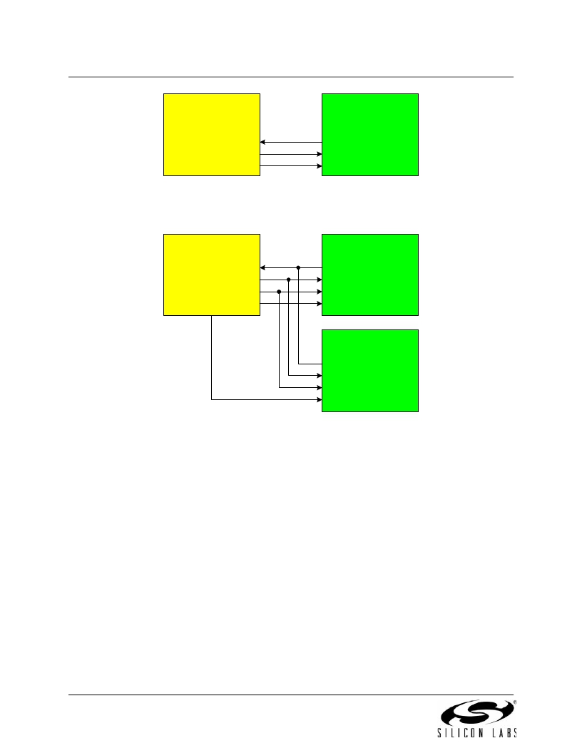
�Figure� 24.4.� 4-Wire� Single� Master� Mode� and� 4-Wire� Slave� Mode� Connection�
�Diagram�
�24.3.� SPI0� Slave� Mode� Operation�
�When� SPI0� is� enabled� and� not� configured� as� a� master,� it� will� operate� as� a� SPI� slave.� As� a� slave,� bytes� are�
�shifted� in� through� the� MOSI� pin� and� out� through� the� MISO� pin� by� a� master� device� controlling� the� SCK� sig-�
�nal.� A� bit� counter� in� the� SPI0� logic� counts� SCK� edges.� When� 8� bits� have� been� shifted� through� the� shift� reg-�
�ister,� the� SPIF� flag� is� set� to� logic� 1,� and� the� byte� is� copied� into� the� receive� buffer.� Data� is� read� from� the�
�receive� buffer� by� reading� SPI0DAT.� A� slave� device� cannot� initiate� transfers.� Data� to� be� transferred� to� the�
�master� device� is� pre-loaded� into� the� shift� register� by� writing� to� SPI0DAT.� Writes� to� SPI0DAT� are� double-�
�buffered,� and� are� placed� in� the� transmit� buffer� first.� If� the� shift� register� is� empty,� the� contents� of� the� transmit�
�buffer� will� immediately� be� transferred� into� the� shift� register.� When� the� shift� register� already� contains� data,�
�the� SPI� will� load� the� shift� register� with� the� transmit� buffer� ’s� contents� after� the� last� SCK� edge� of� the� next� (or�
�current)� SPI� transfer.�
�When� configured� as� a� slave,� SPI0� can� be� configured� for� 4-wire� or� 3-wire� operation.� The� default,� 4-wire�
�slave� mode,� is� active� when� NSSMD1� (SPI0CN.3)� =� 0� and� NSSMD0� (SPI0CN.2)� =� 1.� In� 4-wire� mode,� the�
�NSS� signal� is� routed� to� a� port� pin� and� configured� as� a� digital� input.� SPI0� is� enabled� when� NSS� is� logic� 0,�
�and� disabled� when� NSS� is� logic� 1.� The� bit� counter� is� reset� on� a� falling� edge� of� NSS.� Note� that� the� NSS� sig-�
�nal� must� be� driven� low� at� least� 2� system� clocks� before� the� first� active� edge� of� SCK� for� each� byte� transfer.�
�Figure� 24.4� shows� a� connection� diagram� between� two� slave� devices� in� 4-wire� slave� mode� and� a� master�
�device.�
�160�
�Rev� 1.1�
�相关PDF资料 |
PDF描述 |
|---|---|
| C8051T630DB20 | BOARD SOCKET DAUGHTER 20-QFN |
| CAN-100 | BOARD EVAL RS232 100QFP |
| CANADAPT28 | KIT ADAPTER CANDEMOBOARD 28PLCC |
| CAT24AA01WI-GT3 | IC EEPROM SERIAL 1KB I2C 8SOIC |
| CAT24AA02WI-G | IC EEPROM SERIAL 2KB I2C 8SOIC |
相关代理商/技术参数 |
参数描述 |
|---|---|
| C8051T610DB28 | 功能描述:子卡和OEM板 C8051T610 Family Socket Daughtr Board RoHS:否 制造商:BeagleBoard by CircuitCo 产品:BeagleBone LCD4 Boards 用于:BeagleBone - BB-Bone - Open Source Development Kit |
| C8051T610DB32 | 功能描述:子卡和OEM板 C8051T610 Family Socket Daughtr Board RoHS:否 制造商:BeagleBoard by CircuitCo 产品:BeagleBone LCD4 Boards 用于:BeagleBone - BB-Bone - Open Source Development Kit |
| C8051T610DK | 功能描述:开发板和工具包 - 8051 C8051T610 Series Development Kit RoHS:否 制造商:Silicon Labs 产品:Development Kits 工具用于评估:C8051F960, Si7005 核心: 接口类型:USB 工作电源电压: |
| C8051T610-GQ | 功能描述:8位微控制器 -MCU 16KB 10ADC 32Pin MCU RoHS:否 制造商:Silicon Labs 核心:8051 处理器系列:C8051F39x 数据总线宽度:8 bit 最大时钟频率:50 MHz 程序存储器大小:16 KB 数据 RAM 大小:1 KB 片上 ADC:Yes 工作电源电压:1.8 V to 3.6 V 工作温度范围:- 40 C to + 105 C 封装 / 箱体:QFN-20 安装风格:SMD/SMT |
| C8051T610-GQR | 功能描述:8位微控制器 -MCU 16KB 10ADC 32Pin MCU RoHS:否 制造商:Silicon Labs 核心:8051 处理器系列:C8051F39x 数据总线宽度:8 bit 最大时钟频率:50 MHz 程序存储器大小:16 KB 数据 RAM 大小:1 KB 片上 ADC:Yes 工作电源电压:1.8 V to 3.6 V 工作温度范围:- 40 C to + 105 C 封装 / 箱体:QFN-20 安装风格:SMD/SMT |
发布紧急采购,3分钟左右您将得到回复。