- 您现在的位置:买卖IC网 > Datasheet目录317 > C8051T610DB24 (Silicon Laboratories Inc)DAUGHTER BOARD T610 24QFN SOCKET Datasheet资料下载
参数资料
| 型号: | C8051T610DB24 |
| 厂商: | Silicon Laboratories Inc |
| 文件页数: | 172/218页 |
| 文件大小: | 0K |
| 描述: | DAUGHTER BOARD T610 24QFN SOCKET |
| 标准包装: | 1 |
| 模块/板类型: | QFN 插口模块 |
| 适用于相关产品: | C8051T610DK |
| 相关产品: | 336-1443-ND - KIT DEV FOR C8051T61X MCU'S |
| 其它名称: | 336-1507 |
第1页第2页第3页第4页第5页第6页第7页第8页第9页第10页第11页第12页第13页第14页第15页第16页第17页第18页第19页第20页第21页第22页第23页第24页第25页第26页第27页第28页第29页第30页第31页第32页第33页第34页第35页第36页第37页第38页第39页第40页第41页第42页第43页第44页第45页第46页第47页第48页第49页第50页第51页第52页第53页第54页第55页第56页第57页第58页第59页第60页第61页第62页第63页第64页第65页第66页第67页第68页第69页第70页第71页第72页第73页第74页第75页第76页第77页第78页第79页第80页第81页第82页第83页第84页第85页第86页第87页第88页第89页第90页第91页第92页第93页第94页第95页第96页第97页第98页第99页第100页第101页第102页第103页第104页第105页第106页第107页第108页第109页第110页第111页第112页第113页第114页第115页第116页第117页第118页第119页第120页第121页第122页第123页第124页第125页第126页第127页第128页第129页第130页第131页第132页第133页第134页第135页第136页第137页第138页第139页第140页第141页第142页第143页第144页第145页第146页第147页第148页第149页第150页第151页第152页第153页第154页第155页第156页第157页第158页第159页第160页第161页第162页第163页第164页第165页第166页第167页第168页第169页第170页第171页当前第172页第173页第174页第175页第176页第177页第178页第179页第180页第181页第182页第183页第184页第185页第186页第187页第188页第189页第190页第191页第192页第193页第194页第195页第196页第197页第198页第199页第200页第201页第202页第203页第204页第205页第206页第207页第208页第209页第210页第211页第212页第213页第214页第215页第216页第217页第218页
�� �
�
�C8051T610/1/2/3/4/5/6/7�
�25.1.� Timer� 0� and� Timer� 1�
�Each� timer� is� implemented� as� a� 16-bit� register� accessed� as� two� separate� bytes:� a� low� byte� (TL0� or� TL1)�
�and� a� high� byte� (TH0� or� TH1).� The� Counter/Timer� Control� register� (TCON)� is� used� to� enable� Timer� 0� and�
�Timer� 1� as� well� as� indicate� status.� Timer� 0� interrupts� can� be� enabled� by� setting� the� ET0� bit� in� the� IE� regis-�
�ter� (Section� “16.2.� Interrupt� Register� Descriptions”� on� page� 87);� Timer� 1� interrupts� can� be� enabled� by� set-�
�ting� the� ET1� bit� in� the� IE� register� (Section� “16.2.� Interrupt� Register� Descriptions”� on� page� 87).� Both�
�counter/timers� operate� in� one� of� four� primary� modes� selected� by� setting� the� Mode� Select� bits� T1M1� –� T0M0�
�in� the� Counter/Timer� Mode� register� (TMOD).� Each� timer� can� be� configured� independently.� Each� operating�
�mode� is� described� below.�
�25.1.1.� Mode� 0:� 13-bit� Counter/Timer�
�Timer� 0� and� Timer� 1� operate� as� 13-bit� counter/timers� in� Mode� 0.� The� following� describes� the� configuration�
�and� operation� of� Timer� 0.� However,� both� timers� operate� identically,� and� Timer� 1� is� configured� in� the� same�
�manner� as� described� for� Timer� 0.�
�The� TH0� register� holds� the� eight� MSBs� of� the� 13-bit� counter/timer.� TL0� holds� the� five� LSBs� in� bit� positions�
�TL0.4� –� TL0.0.� The� three� upper� bits� of� TL0� (TL0.7� –� TL0.5)� are� indeterminate� and� should� be� masked� out� or�
�ignored� when� reading.� As� the� 13-bit� timer� register� increments� and� overflows� from� 0x1FFF� (all� ones)� to�
�0x0000,� the� timer� overflow� flag� TF0� in� TCON� is� set� and� an� interrupt� will� occur� if� Timer� 0� interrupts� are�
�enabled.�
�The� C/T0� bit� in� the� TMOD� register� selects� the� counter/timer's� clock� source.� When� C/T0� is� set� to� logic� 1,�
�high-to-low� transitions� at� the� selected� Timer� 0� input� pin� (T0)� increment� the� timer� register� (Refer� to� Section�
�“21.3.� Priority� Crossbar� Decoder”� on� page� 117� for� information� on� selecting� and� configuring� external� I/O�
�pins).� Clearing� C/T� selects� the� clock� defined� by� the� T0M� bit� in� register� CKCON.� When� T0M� is� set,� Timer� 0�
�is� clocked� by� the� system� clock.� When� T0M� is� cleared,� Timer� 0� is� clocked� by� the� source� selected� by� the�
�Clock� Scale� bits� in� CKCON� (see� SFR� Definition� 25.1).�
�Setting� the� TR0� bit� (TCON.4)� enables� the� timer� when� either� GATE0� in� the� TMOD� register� is� logic� 0� or� the�
�input� signal� INT0� is� active� as� defined� by� bit� IN0PL� in� register� IT01CF� (see� SFR� Definition� 16.5).� Setting�
�GATE0� to� 1� allows� the� timer� to� be� controlled� by� the� external� input� signal� INT0� (see� Section� “16.2.� Interrupt�
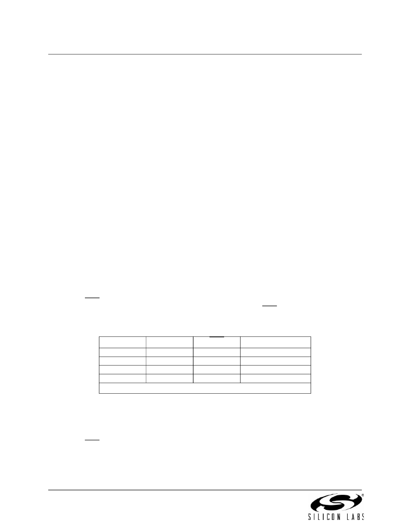
��TR0�
�0�
�1�
�1�
�1�
�GATE0�
�X�
�0�
�1�
�1�
�INT0�
�X�
�X�
�0�
�1�
�Counter/Timer�
�Disabled�
�Enabled�
�Disabled�
�Enabled�
�Note:� X� =� Don't� Care�
�Setting� TR0� does� not� force� the� timer� to� reset.� The� timer� registers� should� be� loaded� with� the� desired� initial�
�value� before� the� timer� is� enabled.�
�TL1� and� TH1� form� the� 13-bit� register� for� Timer� 1� in� the� same� manner� as� described� above� for� TL0� and� TH0.�
�Timer� 1� is� configured� and� controlled� using� the� relevant� TCON� and� TMOD� bits� just� as� with� Timer� 0.� The�
�input� signal� INT0� is� used� with� Timer� 1;� the� /INT1� polarity� is� defined� by� bit� IN1PL� in� register� IT01CF� (see�
�SFR� Definition� 16.5).�
�172�
�Rev� 1.1�
�相关PDF资料 |
PDF描述 |
|---|---|
| C8051T630DB20 | BOARD SOCKET DAUGHTER 20-QFN |
| CAN-100 | BOARD EVAL RS232 100QFP |
| CANADAPT28 | KIT ADAPTER CANDEMOBOARD 28PLCC |
| CAT24AA01WI-GT3 | IC EEPROM SERIAL 1KB I2C 8SOIC |
| CAT24AA02WI-G | IC EEPROM SERIAL 2KB I2C 8SOIC |
相关代理商/技术参数 |
参数描述 |
|---|---|
| C8051T610DB28 | 功能描述:子卡和OEM板 C8051T610 Family Socket Daughtr Board RoHS:否 制造商:BeagleBoard by CircuitCo 产品:BeagleBone LCD4 Boards 用于:BeagleBone - BB-Bone - Open Source Development Kit |
| C8051T610DB32 | 功能描述:子卡和OEM板 C8051T610 Family Socket Daughtr Board RoHS:否 制造商:BeagleBoard by CircuitCo 产品:BeagleBone LCD4 Boards 用于:BeagleBone - BB-Bone - Open Source Development Kit |
| C8051T610DK | 功能描述:开发板和工具包 - 8051 C8051T610 Series Development Kit RoHS:否 制造商:Silicon Labs 产品:Development Kits 工具用于评估:C8051F960, Si7005 核心: 接口类型:USB 工作电源电压: |
| C8051T610-GQ | 功能描述:8位微控制器 -MCU 16KB 10ADC 32Pin MCU RoHS:否 制造商:Silicon Labs 核心:8051 处理器系列:C8051F39x 数据总线宽度:8 bit 最大时钟频率:50 MHz 程序存储器大小:16 KB 数据 RAM 大小:1 KB 片上 ADC:Yes 工作电源电压:1.8 V to 3.6 V 工作温度范围:- 40 C to + 105 C 封装 / 箱体:QFN-20 安装风格:SMD/SMT |
| C8051T610-GQR | 功能描述:8位微控制器 -MCU 16KB 10ADC 32Pin MCU RoHS:否 制造商:Silicon Labs 核心:8051 处理器系列:C8051F39x 数据总线宽度:8 bit 最大时钟频率:50 MHz 程序存储器大小:16 KB 数据 RAM 大小:1 KB 片上 ADC:Yes 工作电源电压:1.8 V to 3.6 V 工作温度范围:- 40 C to + 105 C 封装 / 箱体:QFN-20 安装风格:SMD/SMT |
发布紧急采购,3分钟左右您将得到回复。