- 您现在的位置:买卖IC网 > PDF目录10940 > CS4265-DNZR (Cirrus Logic Inc)IC CODEC 24BIT 104DB 32-QFN PDF资料下载
参数资料
| 型号: | CS4265-DNZR |
| 厂商: | Cirrus Logic Inc |
| 文件页数: | 21/46页 |
| 文件大小: | 0K |
| 描述: | IC CODEC 24BIT 104DB 32-QFN |
| 标准包装: | 6,000 |
| 类型: | 立体声音频 |
| 数据接口: | 串行 |
| 分辨率(位): | 24 b |
| ADC / DAC 数量: | 2 / 2 |
| 三角积分调变: | 是 |
| 动态范围,标准 ADC / DAC (db): | 104 / 104 |
| 电压 - 电源,模拟: | 3.13 V ~ 5.25 V |
| 电压 - 电源,数字: | 3.13 V ~ 5.25 V |
| 工作温度: | -40°C ~ 105°C |
| 安装类型: | 表面贴装 |
| 封装/外壳: | 32-QFN |
| 供应商设备封装: | 32-QFN 裸露焊盘(5x5) |
| 包装: | 带卷 (TR) |
| 配用: | 598-1001-ND - BOARD EVAL FOR CS4265 CODEC |
第1页第2页第3页第4页第5页第6页第7页第8页第9页第10页第11页第12页第13页第14页第15页第16页第17页第18页第19页第20页当前第21页第22页第23页第24页第25页第26页第27页第28页第29页第30页第31页第32页第33页第34页第35页第36页第37页第38页第39页第40页第41页第42页第43页第44页第45页第46页
28
DS657F3
CS4265
topology. If pseudo-differential input functionality is not required, simply connect the SGND pin to AGND
through the parallel combination of a 10 F and a 0.1 F capacitor.
4.6
Output Connections
The CS4265 DACs implement a switched-capacitor filter, followed by a continuous time low-pass filter. Its
response, combined with tha t of the digital interpolator, is sh own in Section 8. “DAC Filter Plots” on
page 48”. The recommended external analog circuitry is shown in the Typical Connection Diagram.
The CS4265 DAC does not include phase or amplitude compensation for an external filter. Therefore, the
DAC system phase and amplitude response is dependent on the external analog circuitry.
4.7
Output Transient Control
The CS4265 uses Popguard technology to minimize the effects of output transients during power-up and
power-down. This technique eliminates the audio transients commonly produced by single-ended, single-
supply converters when it is implemented with external DC-blocking capacitors connected in series with the
audio outputs. To make best use of this feature, it is necessary to understand its operation.
4.7.1
Power-Up
When the device is initially powered-up, the DAC outputs AOUTA and AOUTB are clamped to VQ, which
is initially low. After the PDN bit is released (set to ‘0’), the outputs begin to ramp with VQ towards the
nominal quiescent voltage. This ramp takes approximately 200 ms to complete. The gradual voltage
ramping allows time for the external DC-blocking capacitors to charge to VQ, effectively blocking the qui-
escent DC voltage. Audio output will begin after approximately 2000 sample periods.
4.7.2
Power-Down
To prevent audio transients at power-down, the DC-blocking capacitors must fully discharge before turn-
ing off the power. In order to do this, either the PDN should be set or the device should be reset about
250 ms before removing power. During this time, the voltage on VQ and the DAC outputs will gradually
discharge to GND. If power is removed before this 250 ms time period has passed, a transient will occur
when the VA supply drops below that of VQ. There is no minimum time for a power cycle; power may be
re-applied at any time.
4.7.3
Serial Interface Clock Changes
When changing the clock ratio or sample rate, it is recommended that zero data (or near zero data) be
present on the selected SDIN pin for at least 10 LRCK samples before the change is made. During the
+
-
VA
+
-
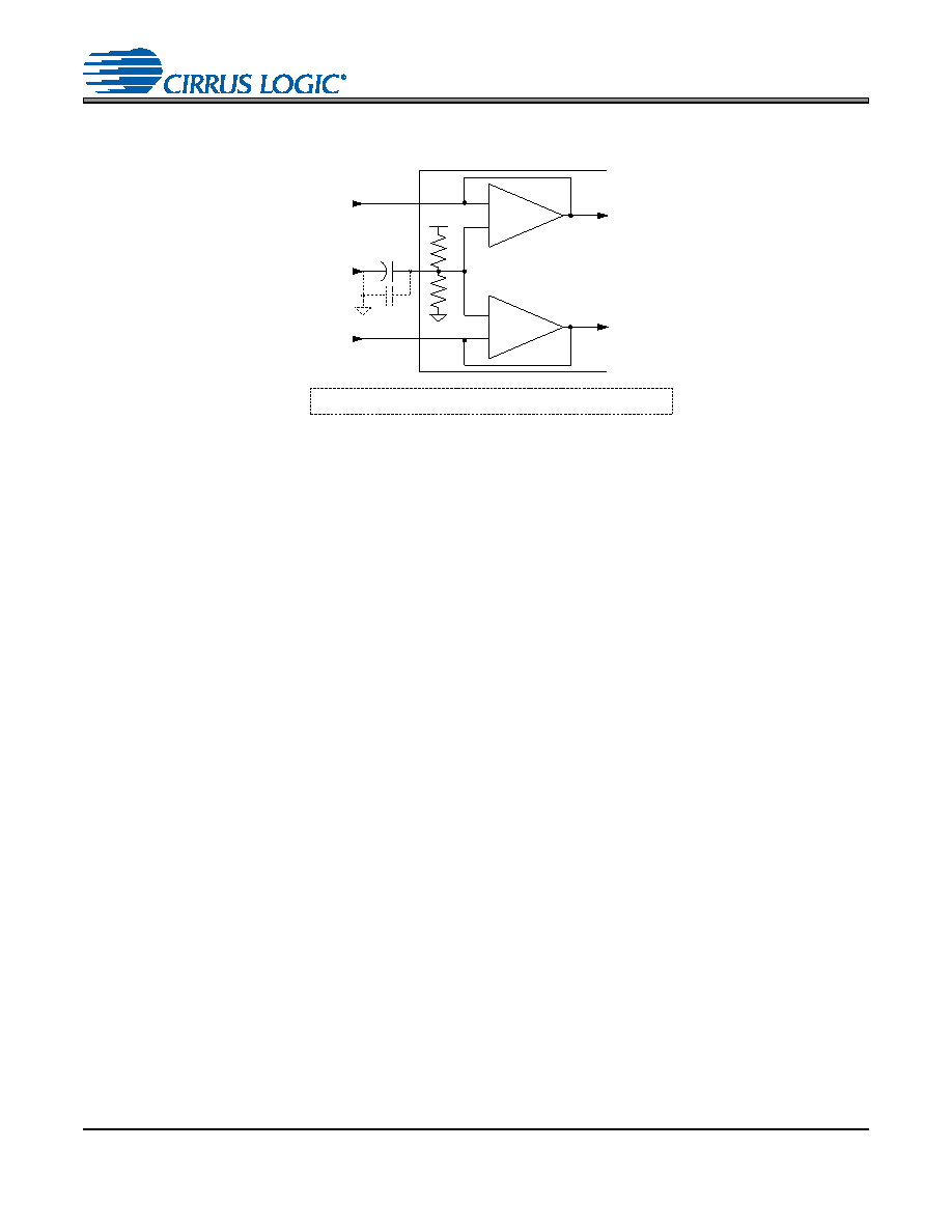
AINA
AINB
SG ND
In to PG A
10 F
0.1 F
Note: If pseudo-differential input functionality is not required, the
connections shown with dashed line should be added.
Figure 12. Pseudo-Differential Input Stage
CS4265
相关PDF资料 |
PDF描述 |
|---|---|
| VE-J3H-IX-S | CONVERTER MOD DC/DC 52V 75W |
| VE-J3D-IX-S | CONVERTER MOD DC/DC 85V 75W |
| ADAU1381BCBZ-RL7 | IC AUDIO CODEC STEREO LN 30WLCSP |
| ADAU1381BCBZ-RL | IC AUDIO CODEC STEREO LN 30WLCSP |
| VI-B3K-IW-B1 | CONVERTER MOD DC/DC 40V 100W |
相关代理商/技术参数 |
参数描述 |
|---|---|
| CS4267AM | 制造商:Rochester Electronics LLC 功能描述:- Bulk |
| CS4270 | 制造商:CIRRUS 制造商全称:Cirrus Logic 功能描述:24-Bit, 192 kHz Stereo Audio CODEC |
| CS4270_06 | 制造商:CIRRUS 制造商全称:Cirrus Logic 功能描述:24-Bit, 192 kHz Stereo Audio CODEC |
| CS4270-CZZ | 功能描述:接口—CODEC Stereo Audio CODEC 105 dB 192 kHz RoHS:否 制造商:Texas Instruments 类型: 分辨率: 转换速率:48 kSPs 接口类型:I2C ADC 数量:2 DAC 数量:4 工作电源电压:1.8 V, 2.1 V, 2.3 V to 5.5 V 最大工作温度:+ 85 C 安装风格:SMD/SMT 封装 / 箱体:DSBGA-81 封装:Reel |
| CS4270-CZZR | 功能描述:接口—CODEC IC 105dB 192kHz Stereo Codec RoHS:否 制造商:Texas Instruments 类型: 分辨率: 转换速率:48 kSPs 接口类型:I2C ADC 数量:2 DAC 数量:4 工作电源电压:1.8 V, 2.1 V, 2.3 V to 5.5 V 最大工作温度:+ 85 C 安装风格:SMD/SMT 封装 / 箱体:DSBGA-81 封装:Reel |
发布紧急采购,3分钟左右您将得到回复。