- 您现在的位置:买卖IC网 > PDF目录9597 > CY28317PVXC-2T (Silicon Laboratories Inc)IC CLK FTG VIA PL/E133T 48SSOP PDF资料下载
参数资料
| 型号: | CY28317PVXC-2T |
| 厂商: | Silicon Laboratories Inc |
| 文件页数: | 7/20页 |
| 文件大小: | 0K |
| 描述: | IC CLK FTG VIA PL/E133T 48SSOP |
| 标准包装: | 1,000 |
| 类型: | 时钟/频率发生器 |
| PLL: | 是 |
| 输入: | 晶体 |
| 输出: | HCSL,LVCMOS |
| 电路数: | 1 |
| 比率 - 输入:输出: | 1:20 |
| 差分 - 输入:输出: | 无/是 |
| 频率 - 最大: | 248MHz |
| 电源电压: | 3.135 V ~ 3.465 V |
| 工作温度: | 0°C ~ 70°C |
| 安装类型: | 表面贴装 |
| 封装/外壳: | 48-BSSOP(0.295",7.50mm 宽) |
| 供应商设备封装: | 48-SSOP |
| 包装: | 带卷 (TR) |
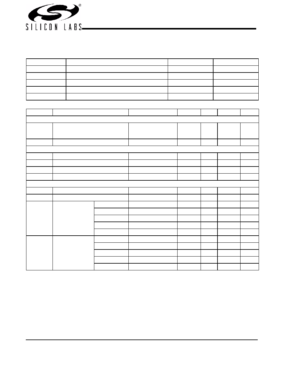
CY28317-2
..................... Document #: 38-07094 Rev. *B Page 15 of 20
Absolute Maximum Ratings[2]
Stresses greater than those listed in this table may cause permanent damage to the device. These represent a stress rating only.
Operation of the device at these or any other conditions above those specified in the operating sections of this specification is
not implied. Maximum conditions for extended periods may affect reliability.
Parameter
Description
Rating
Unit
VDD, VIN
Voltage on any pin with respect to GND
–0.5 to +7.0
V
TSTG
Storage Temperature
–65 to +150
°C
TB
Ambient Temperature under Bias
–55 to +125
°C
TA
Operating Temperature
0 to +70
°C
ESDPROT
Input ESD Protection
2 (min.)
kV
DC Electrical Characteristics: TA = 0°C to +70°C, VDDQ3 = 3.3V ±5%
[3]
Parameter
Description
Test Condition
Min.
Typ.
Max.
Unit
Supply Current
IDD3
3.3V Supply Current
VDD = 3.465V,
FCPU = 133 MHz
250
mA
IDDPD3
3.3V Shut down Current
VDD = 3.465V
25
mA
Logic Inputs
VIL
Input Low Voltage
GND – 0.3
0.8
V
VIH
Input High Voltage
2.0
VDD + 0.3
V
IIL
Input Low Current[4]
–25
A
IIH
Input High Current[4]
10
A
Clock Outputs
VOL
Output Low Voltage
IOL = 1 mA
50
mV
VOH
Output High Voltage
IOH = –1 mA
3.1
V
IOL
Output Low Current
PCI0:5
VOL = 1.5V
70
110
135
mA
REF0:1
VOL = 1.5V
50
70
100
mA
48 MHz
VOL = 1.5V
50
70
100
mA
24 MHz
VOL = 1.5V
50
70
100
mA
SDRAM
VOL = 1.5V
70
110
135
mA
IOH
Output High Current
PCI0:5
VOH = 1.5V
70
110
135
mA
REF0:1
VOH = 1.5V
50
70
100
mA
48 MHz
VOH = 1.5V
50
70
100
mA
24 MHz
VOH = 1.5V
50
70
100
mA
SDRAM
VOH = 1.5V
70
110
135
mA
Notes:
2. The voltage on any input or I/O pin cannot exceed the power pin during power-up. Power supply sequencing is NOT required.
3. All clock outputs loaded with 6" 60
transmission lines with 20-pF capacitors.
4. CY28317-2 logic inputs (except FS3) have internal pull-up devices (pull-ups not full CMOS level). Logic input FS3 has an internal pull-down device.
相关PDF资料 |
PDF描述 |
|---|---|
| D38999/24WG11SC | CONN RCPT 11POS JAM NUT W/SCKT |
| V48B2H100B3 | CONVERTER MOD DC/DC 2V 100W |
| IDTCSPT857DPAGI | IC PLL CLK DVR SDRAM 48-TSSOP |
| MS3111P20-41S | CONN RCPT 41POS CBL MNT W/SCKT |
| V48B28H250BL | CONVERTER MOD DC/DC 28V 250W |
相关代理商/技术参数 |
参数描述 |
|---|---|
| CY28317ZC-2 | 制造商:CYPRESS 制造商全称:Cypress Semiconductor 功能描述:FTG for Mobile VIA PL133T and PLE133T Chipsets |
| CY28317ZC-2T | 制造商:CYPRESS 制造商全称:Cypress Semiconductor 功能描述:FTG for Mobile VIA PL133T and PLE133T Chipsets |
| CY28322 | 制造商:未知厂家 制造商全称:未知厂家 功能描述:Clocks and Buffers |
| CY28322-2 | 制造商:CYPRESS 制造商全称:Cypress Semiconductor 功能描述:133-MHz Spread Spectrum Clock Synthesizer with Differential CPU Outputs |
| CY28322ZC-2 | 制造商:Rochester Electronics LLC 功能描述:- Bulk |
发布紧急采购,3分钟左右您将得到回复。