- 您现在的位置:买卖IC网 > PDF目录9582 > CY28446LFXCT (Silicon Laboratories Inc)IC CLOCK CALISTOGA CK410M 64QFN PDF资料下载
参数资料
| 型号: | CY28446LFXCT |
| 厂商: | Silicon Laboratories Inc |
| 文件页数: | 13/19页 |
| 文件大小: | 0K |
| 描述: | IC CLOCK CALISTOGA CK410M 64QFN |
| 标准包装: | 2,000 |
| 类型: | 时钟/频率发生器 |
| PLL: | 是 |
| 主要目的: | Intel CPU 服务器 |
| 输入: | LVTTL,晶体 |
| 输出: | HCSL,LVCMOS |
| 电路数: | 1 |
| 比率 - 输入:输出: | 3:20 |
| 差分 - 输入:输出: | 无/是 |
| 频率 - 最大: | 200MHz |
| 电源电压: | 3.135 V ~ 3.465 V |
| 工作温度: | 0°C ~ 70°C |
| 安装类型: | 表面贴装 |
| 封装/外壳: | 64-VFQFN 裸露焊盘 |
| 供应商设备封装: | 64-QFN(9x9) |
| 包装: | 带卷 (TR) |
CY28446
.......................Document #: 001-00168 Rev *F Page 3 of 19
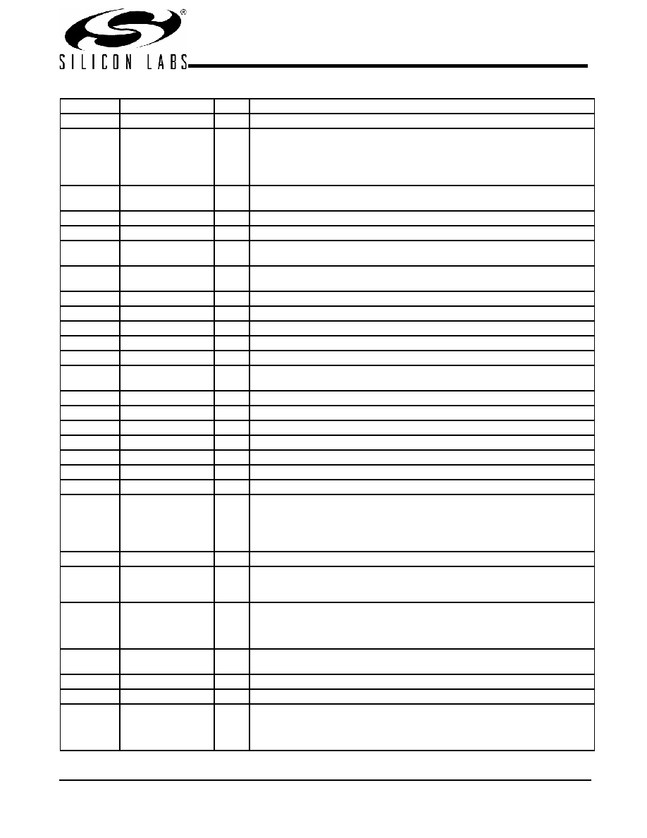
Pin Description
Pin No.
Name
Type
Description
1VSS_48
GND
Ground for outputs.
2, 3, 5, 6, 8,
9, 13, 14, 18,
19, 20, 21,
22, 23, 25,
26, 27, 28
SRC(0:3, 5:6, 8:10)
[T/C]
O, DIF 100 MHz Differential serial reference clocks
4, 7, 12, 15,
24, 64
OE[0, 1, 3, 6, A, B]#
I, PU
3.3V LVTTL input for enabling assigned SRC clock (active LOW)
10, 17, 29,
VDD_SRC
PWR 3.3V power supply for outputs.
11, 30, 33
VSS_SRC
GND
Ground for outputs.
16
PCI_STP#
I, PU
3.3V LVTTL input for PCI_STP#
Stops SRC and PCI clocks not set to free running in the SMBUS registers.
31, 32
CPU2_ITPT/SRCT7,
CPU2_ITPC/SRCC7
O, DIF Selectable differential CPU clock/100 MHz Differential serial reference clock.
Selectable via Pin 53 PCIF0/ITP_EN
34, 35, 38, 39 CPUT/C[0:1]
O, DIF Differential CPU clock outputs.
36
VDD_CPU
PWR 3.3V power supply for outputs.
37
VSS_CPU
GND
Ground for outputs.
40
CPU_STP#
I, PU
3.3V LVTTL input for CPU_STP# active LOW.
41
SCLK
I
SMBus-compatible SCLOCK.
42
SDATA
I/O,
OD
SMBus-compatible SDATA.
43
VDD_REF
PWR 3.3V power supply for outputs.
44
XOUT
O, SE 14.318 MHz crystal output.
45
XIN
I
14.318 MHz crystal input.
46
VSS_REF
GND
Ground for outputs.
47
REF
O,SE Fixed 14.318 MHz clock output.
48, 54
VDD_PCI
PWR 3.3V power supply for outputs.
49, 50, 51, 52 PCI[0:3]
O, SE 33 MHz clock output
53
PCIF0/ITP_EN
I/O, PD 33 MHz clock output (not stoppable by PCI_STOP#)/3.3V LVTTL input for
selecting pins 31/32 (CPU2_ITP[T/C]/SRC7[T/C]) (sampled on the
VTT_PWRGD# assertion).
0 (default): SRC7[T/C]
1: CPU2_ITP[T/C]
55, 59
VSS_PCI
GND
Ground for outputs.
56
VTT_PWRGD#/PD
I, PD
3.3V LVTTL input. This pin is a level sensitive strobe used to latch the FS_A, FS_B,
FS_C, and all I/O configuration pins,. After VTT_PWRGD# (active LOW) assertion,
this pin becomes a real-time input for asserting power-down (active HIGH).
57
FS_C/TEST_SEL
I, PD
3.3V-tolerant input for CPU frequency selection/Selects test mode if pulled to
VIMFS_C when VTT_PWRGD# is asserted LOW.
Refer to DC Electrical Specifications table for VILFS_C,VIMFS_C,VIHFS_C specifica-
tions.
58
USB_48/FS_A
I/O, PU Fixed 48 MHz clock output/3.3V-tolerant input for CPU frequency selection.
Refer to DC Electrical Specifications table for Vil_FS and Vih_FS specifications.
60
VDD_48
PWR 3.3V power supply for outputs.
61,62
DOT_96[T/C]
O, DIF Fixed 96 MHz clock output.
63
FS_B/TEST_MODE
I, PU
3.3V-tolerant input for CPU frequency selection Selects Ref/N or Tri-state
when in test mode
0 = Tri-state, 1 = Ref/N
Refer to DC Electrical Specifications table for Vil_FS and Vih_FS specifications.
相关PDF资料 |
PDF描述 |
|---|---|
| CY28445LFXC-5T | IC CLOCK CALISTOGA CK410M 68QFN |
| VI-B4J-IU | CONVERTER MOD DC/DC 36V 200W |
| MC1489DR2G | IC LINE RECEIVER QUAD 14-SOIC |
| VI-B4F-IU | CONVERTER MOD DC/DC 72V 200W |
| VI-B31-MY-S | CONVERTER MOD DC/DC 12V 50W |
相关代理商/技术参数 |
参数描述 |
|---|---|
| CY28447 | 制造商:SPECTRALINEAR 制造商全称:SPECTRALINEAR 功能描述:Clock Generator for Intel㈢ Calistoga Chipset |
| CY28447LFXC | 功能描述:时钟发生器及支持产品 Calistoga System Clk Extra SRC Output RoHS:否 制造商:Silicon Labs 类型:Clock Generators 最大输入频率:14.318 MHz 最大输出频率:166 MHz 输出端数量:16 占空比 - 最大:55 % 工作电源电压:3.3 V 工作电源电流:1 mA 最大工作温度:+ 85 C 安装风格:SMD/SMT 封装 / 箱体:QFN-56 |
| CY28447LFXCT | 功能描述:时钟发生器及支持产品 Calistoga System Clk Extra SRC Output RoHS:否 制造商:Silicon Labs 类型:Clock Generators 最大输入频率:14.318 MHz 最大输出频率:166 MHz 输出端数量:16 占空比 - 最大:55 % 工作电源电压:3.3 V 工作电源电流:1 mA 最大工作温度:+ 85 C 安装风格:SMD/SMT 封装 / 箱体:QFN-56 |
| CY28506OC | 制造商:Rochester Electronics LLC 功能描述:FTG FOR MOTHERBOARDS - Bulk |
| CY28506OCT | 制造商:Rochester Electronics LLC 功能描述:CLOC - Tape and Reel |
发布紧急采购,3分钟左右您将得到回复。