- 您现在的位置:买卖IC网 > PDF目录256924 > CY38015V208-83NI (CYPRESS SEMICONDUCTOR CORP) LOADABLE PLD, 15 ns, PQFP208 PDF资料下载
参数资料
| 型号: | CY38015V208-83NI |
| 厂商: | CYPRESS SEMICONDUCTOR CORP |
| 元件分类: | PLD |
| 英文描述: | LOADABLE PLD, 15 ns, PQFP208 |
| 封装: | PLASTIC, QFP-208 |
| 文件页数: | 31/32页 |
| 文件大小: | 929K |
| 代理商: | CY38015V208-83NI |
第1页第2页第3页第4页第5页第6页第7页第8页第9页第10页第11页第12页第13页第14页第15页第16页第17页第18页第19页第20页第21页第22页第23页第24页第25页第26页第27页第28页第29页第30页当前第31页第32页
PRELIMINARY
Quantum38K ISR
CPLD Family
Document #: 38-03043 Rev. **
Page 8 of 32
Channel Memory Routing Interface
Similar to LBC outputs, the channel memory blocks feature
dedicated tracks in the horizontal and vertical routing channels
for the data outputs and the flag outputs, as shown in Figure
5. This allows the channel memory blocks to be expanded
easily. These dedicated lines can be routed to I/O pins as chip
outputs or to other logic block clusters to be used in logic equa-
tions.
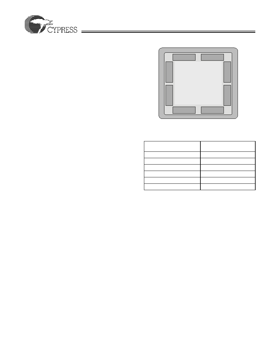
I/O Banks
The Quantum38K interfaces the horizontal and vertical routing
channels to the pins through I/O banks. There are 8 I/O banks
per device as shown in Figure 6, and all I/Os from an I/O bank
are located in the same section of a package for PCB layout
convenience.
For each package type, Quantum38K devices of different den-
sities keep given pins in the same I/O banks. This supports
and simplifies design migration across densities.
Each I/O bank contains several I/O cells, and each I/O cell
contains an input/output register, an output enable register,
programmable slew rate control and programmable bus hold
control logic. Each I/O cell drives a pin output of the device;
the cell also supplies an input to the device that connects to a
dedicated track in the associated routing channel.
There are four dedicated inputs (GCTL[3:0]) that are used as
Global Control Signals available to every I/O cell. These global
control signals may be used as output enables, register resets
and register clock enables as shown in Figure 7.
Each I/O bank can use any supported I/O standard by supply-
ing appropriate VCCIO voltages. All the VCCIO pins in an I/O
bank must be connected to the same VCCIO voltage. This re-
quirement restricts the number of I/O standards supported by
an I/O bank at any given time.
Figure 6. Quantum38K I/O Bank Block Diagram
.
IO Standards
I/O
Standard
VCCIO
LVTTL
3.3V
LVCMOS
3.3V
LVCMOS3
3.0V
LVCMOS2
2.5V
LVCMOS18
1.8V
3.3V PCI
3.3V
Delta39K
bank
0
bank
1
bank
4
bank
5
bank 2
bank 3
bank 6
bank 7
Quantum38K
相关PDF资料 |
PDF描述 |
|---|---|
| CY38015V256-66BBC | LOADABLE PLD, 18.9 ns, PBGA256 |
| CY38015V256-66BBI | LOADABLE PLD, 18.9 ns, PBGA256 |
| CY38015V256-83BBC | LOADABLE PLD, 15 ns, PBGA256 |
| CY38015V256-83BBI | LOADABLE PLD, 15 ns, PBGA256 |
| CP21600CPGA383A-0C | FPGA, 2940 CLBS, 13700 GATES, CPGA383 |
相关代理商/技术参数 |
参数描述 |
|---|---|
| CY38050V208-125NTC | 制造商:Cypress Semiconductor 功能描述:CPLD QUANTUM38K 72K GATES 768 MCRCLLS COMM 0.18UM 2.5V/3.3V - Bulk |
| CY38050V208-125NTI | 制造商:Cypress Semiconductor 功能描述:CPLD QUANTUM38K 72K GATES 768 MCRCLLS IND 0.18UM 2.5V/3.3V 2 - Bulk |
| CY38050V208-83NTC | 制造商:Cypress Semiconductor 功能描述:CPLD QUANTUM38K 72K GATES 768 MCRCLLS COMM 0.18UM 2.5V/3.3V - Bulk |
| CY38050V208-83NTI | 制造商:Cypress Semiconductor 功能描述:CPLD QUANTUM38K 72K GATES 768 MCRCLLS IND 0.18UM 2.5V/3.3V 2 - Bulk |
| CY38100V208-125NTI | 制造商:Cypress Semiconductor 功能描述:CPLD QUANTUM38K 144K GATES 1536 MCRCLLS IND 0.18UM 2.5V/3.3V - Bulk |
发布紧急采购,3分钟左右您将得到回复。