- 您现在的位置:买卖IC网 > PDF目录223638 > CY7C1371BV25-83BGC (CYPRESS SEMICONDUCTOR CORP) 512K X 36 ZBT SRAM, 10 ns, PBGA119 PDF资料下载
参数资料
| 型号: | CY7C1371BV25-83BGC |
| 厂商: | CYPRESS SEMICONDUCTOR CORP |
| 元件分类: | SRAM |
| 英文描述: | 512K X 36 ZBT SRAM, 10 ns, PBGA119 |
| 封装: | 14 X 22 MM, 2.40 MM HEIGHT, PLASTIC, BGA-119 |
| 文件页数: | 9/25页 |
| 文件大小: | 709K |
| 代理商: | CY7C1371BV25-83BGC |
CY7C1373BV25
CY7C1371BV25
Document #: 38-05250 Rev. *A
Page 17 of 25
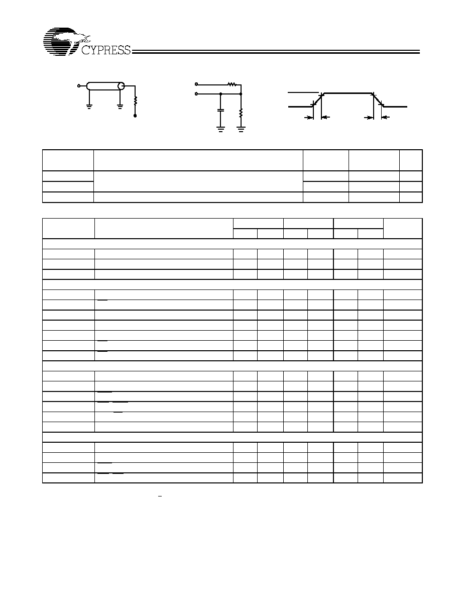
AC Test Loads and Waveforms
Thermal Resistance[15]
Description
Test Conditions
QJA
(Junction to Am-
bient)
QJC
(Junction to Case)
Units
119-ball BGA
Still Air, soldered on a 114.3 × 101.6 × 1.57 mm3, 2-layer board
41.54
6.33
°C/W
165-ball FBGA
44.51
2.38
°C/W
100-pin TQFP
Still Air, soldered on a 4.25 × 1.125 inch, 4-layer printed circuit board
25
9
°C/W
OUTPUT
R = 1667
R = 1538
5pF
Including
Jig and
Scope
(a)
(b)
OUTPUT
RL = 50
Z0 = 50
VL = 1.25V
VDDQ
ALL INPUT PULSES
[17]
2.5V
GND
90%
10%
90%
10%
≤ 2.0 ns
(c)
Switching Characteristics Over the Operating Range [18]
Parameter
Description
117
100
83
Unit
Min.
Max.
Min.
Max.
Min.
Max.
Clock
tCYC
Clock Cycle Time
8.5
10.0
12
ns
tCH
Clock HIGH
2.3
2.5
3.0
ns
tCL
Clock LOW
2.3
2.5
3.0
ns
Output Times
tCDV
Data Output Valid After CLK Rise
7.5
8.5
10.0
ns
tEOV
OE LOW to Output Valid[15, 21]
3.4
3.8
4.2
ns
tDOH
Data Output Hold After CLK Rise
1.3
ns
tCHZ
Clock to High-Z[19, 20, 21]
3.0
ns
tCLZ
Clock to Low-Z[19, 20, 21]
1.3
ns
tEOHZ
OE HIGH to Output High-Z[19, 20, 21]
4.0
ns
tEOLZ
OE LOW to Output Low-Z[19, 20, 21]
00
0
ns
Set-up Times
tAS
Address Set-up Before CLK Rise
1.5
ns
tDS
Data Input Set-up Before CLK Rise
1.5
ns
tCENS
CEN Set-up Before CLK Rise
1.5
ns
tWES
WE, BWSx Set-up Before CLK Rise
1.5
ns
tALS
ADV/LD Set-up Before CLK Rise
1.5
ns
tCES
Chip Select Set-up
1.5
ns
Hold Times
tAH
Address Hold After CLK Rise
0.5
ns
tDH
Data Input Hold After CLK Rise
0.5
ns
tCENH
CEN Hold After CLK Rise
0.5
ns
tWEH
WE, BWx Hold After CLK Rise
0.5
ns
Notes:
17. Input waveform should have a slew rate of <1 V/ns.
18. Unless otherwise noted, test conditions assume signal transition time of 2.5 ns or less, timing reference levels of 1.25V, input pulse levels of 0 to 2.5V, and
output loading of the specified IOL/IOH and load capacitance. Shown in (a), (b) and (c) of AC Test Loads.
19. tCHZ, tCLZ, tOEV, tEOLZ, and tEOHZ are specified with AC test conditions shown in part (a) of AC Test Loads. Transition is measured ± 200 mV from steady-state
voltage.
20. At any given voltage and temperature, tEOHZ is less than tEOLZ and tCHZ is less than tCLZ to eliminate bus contention between SRAMs when sharing the same
data bus. These specifications do not imply a bus contention condition, but reflect parameters guaranteed over worst case user conditions. Device is designed
to achieve High-Z prior to Low-Z under the same system conditions.
21. This parameter is sampled and not 100% tested.
相关PDF资料 |
PDF描述 |
|---|---|
| CY7C341B-25JC | OT PLD, 40 ns, PQCC84 |
| CY7C341B-25JI | OT PLD, 40 ns, PQCC84 |
| CY7C341B-35JC | OT PLD, 55 ns, PQCC84 |
| CY7C341B-35JI | OT PLD, 55 ns, PQCC84 |
| CY7C341B-25RC | UV PLD, 40 ns, CPGA84 |
相关代理商/技术参数 |
参数描述 |
|---|---|
| CY7C1371C-100AC | 功能描述:IC SRAM 18MBIT 100MHZ 100LQFP RoHS:否 类别:集成电路 (IC) >> 存储器 系列:- 标准包装:96 系列:- 格式 - 存储器:闪存 存储器类型:FLASH 存储容量:16M(2M x 8,1M x 16) 速度:70ns 接口:并联 电源电压:2.65 V ~ 3.6 V 工作温度:-40°C ~ 85°C 封装/外壳:48-TFSOP(0.724",18.40mm 宽) 供应商设备封装:48-TSOP 包装:托盘 |
| CY7C1371C-100AIT | 制造商:Cypress Semiconductor 功能描述:SRAM Chip Sync Quad 3.3V 18M-Bit 512K x 36 8.5ns 100-Pin TQFP T/R |
| CY7C1371C-100BZC | 制造商:Rochester Electronics LLC 功能描述:16MB (512KX36) 3.3V NOBL-FT SRAM - Bulk 制造商:Cypress Semiconductor 功能描述: |
| CY7C1371C-117BGC | 制造商:Cypress Semiconductor 功能描述:SRAM Chip Sync Quad 3.3V 18M-Bit 512K x 36 7.5ns 119-Pin BGA 制造商:Cypress Semiconductor 功能描述:SRAM Chip Sync Single 3.3V 18M-Bit 512K x 36 7.5ns 119-Pin BGA 制造商:Rochester Electronics LLC 功能描述:16MB (512KX36) 3.3V NOBL-FT SRAM - Bulk |
| CY7C1371C-133BGC | 制造商:Rochester Electronics LLC 功能描述:16MB (512KX36) 3.3V NOBL-FT SRAM - Bulk 制造商:Cypress Semiconductor 功能描述: |
发布紧急采购,3分钟左右您将得到回复。