- 您现在的位置:买卖IC网 > PDF目录223638 > CY7C341B-25RI (CYPRESS SEMICONDUCTOR CORP) UV PLD, 40 ns, CPGA84 PDF资料下载
参数资料
| 型号: | CY7C341B-25RI |
| 厂商: | CYPRESS SEMICONDUCTOR CORP |
| 元件分类: | PLD |
| 英文描述: | UV PLD, 40 ns, CPGA84 |
| 封装: | WINDOWED, PGA-84 |
| 文件页数: | 7/12页 |
| 文件大小: | 339K |
| 代理商: | CY7C341B-25RI |
USE ULTRA37000 FOR
ALL NEW DESIGNS
CY7C341B
Document #: 38-03016 Rev. *C
Page 4 of 12
Logic Array Blocks
There are 12 logic array blocks in the CY7C341B. Each LAB
consists of a macrocell array containing 16 macrocells, an
expander product term array containing 32 expanders, and an
I/O block. The LAB is fed by the programmable interconnect
array and the dedicated input bus. All macrocell feedbacks go
to the macrocell array, the expander array, and the program-
mable interconnect array. Expanders feed themselves and the
macrocell array. All I/O feedbacks go to the programmable
interconnect array so that they may be accessed by macro-
cells in other LABs as well as the macrocells in the LAB in
which they are situated.
Externally, the CY7C341B provides eight dedicated inputs,
one of which may be used as a system clock. There are 64 I/O
pins that may be individually configured for input, output, or
bidirectional data flow.
Programmable Interconnect Array
The Programmable Interconnect Array (PIA) solves inter-
connect limitations by routing only the signals needed by each
logic array block. The inputs to the PIA are the outputs of every
macrocell within the device and the I/O pin feedback of every
pin on the device.
Unlike masked or programmable gate arrays, which induce
variable delay dependent on routing, the PIA has a fixed delay.
This eliminates undesired skews among logic signals, which
may cause glitches in internal or external logic. The fixed
delay, regardless of programmable interconnect array config-
uration, simplifies design by assuring that internal signal
skews or races are avoided. The result is ease of design imple-
mentation, often in a single pass, without the multiple internal
logic placement and routing iterations required for a program-
mable gate array to achieve design timing objectives.
Design Recommendations
For proper operation, input and output pins must be
constrained to the range GND < (VIN or VOUT) < VCC.
Unused inputs must always be tied to an appropriate logic
level (either VCC or GND). Each set of VCC and GND pins
must be connected together directly at the device. Power
supply decoupling capacitors of at least 0.2 mF must be
connected between VCC and GND. For the most effective
decoupling, each VCC pin should be separately decoupled to
GND, directly at the device. Decoupling capacitors should
have good frequency response, such as monolithic ceramic
types.
Design Security
The CY7C341B contains a programmable design security
feature that controls the access to the data programmed into
the device. If this programmable feature is used, a proprietary
design implemented in the device cannot be copied or
retrieved. This enables a high level of design control to be
obtained since programmed data within EPROM cells is
invisible. The bit that controls this function, along with all other
program data, may be reset simply by erasing the device.
The CY7C341B is fully functionally tested and guaranteed
through complete testing of each programmable EPROM bit
and
all
internal
logic
elements
thus
ensuring
100%
programming yield.
The erasable nature of these devices allows test programs to
be used and erased during early stages of the production flow.
The devices also contain on-board logic test circuitry to allow
verification of function and AC specification once encapsu-
lated in non-windowed packages.
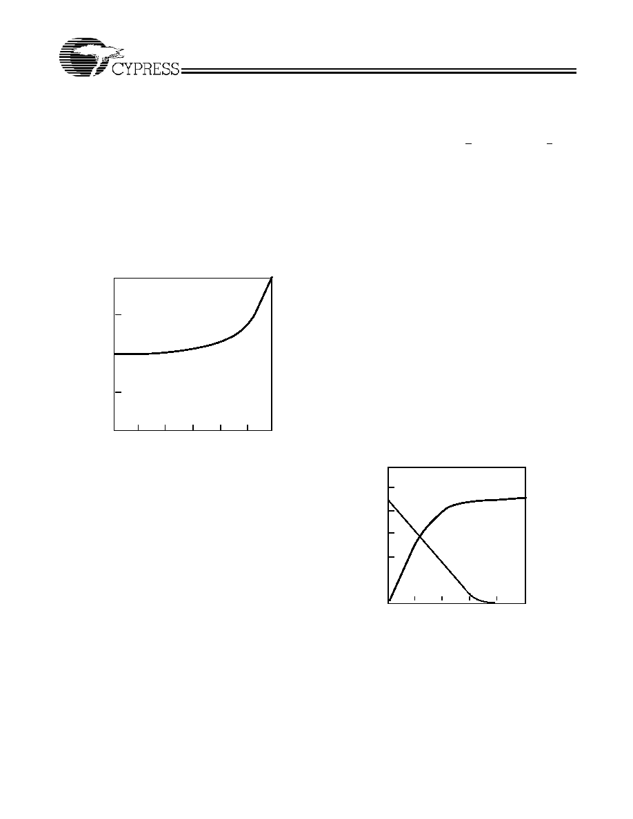
400
300
200
100
1 kHz
10 kHz
100 kHz
1 MHz
I CC
MAXIMUM FREQUENCY
10 MHz
0
50 MHz
100 Hz
ACTIVE
(mA)
Typ.
VCC = 5.0V
Room Temp.
Typical ICC vs. fMAX
01
2
3
4
I
OU
T
P
UT
CU
RR
E
N
T
(m
A
)T
Y
PI
CA
L
VO OUTPUTVOLTAGE (V)
250
200
150
100
50
5
O
IOH
IOL
VCC = 5.0V
Room Temp.
Output Drive Current
相关PDF资料 |
PDF描述 |
|---|---|
| CY7C341B-35RC | UV PLD, 55 ns, CPGA84 |
| CY7C341B-35RI | UV PLD, 55 ns, CPGA84 |
| CY7C341B-25HC | UV PLD, 40 ns, CQCC84 |
| CY7C341B-25HI | UV PLD, 40 ns, CQCC84 |
| CY7C341B-35HC | UV PLD, 55 ns, CQCC84 |
相关代理商/技术参数 |
参数描述 |
|---|---|
| CY7C341B-35JI | 制造商:Cypress Semiconductor 功能描述:CPLD MAX 制造商:QP Semiconductor 功能描述:7C341B CYP DIE 35NS-PLCC |
| CY7C341B-35RI | 制造商:Cypress Semiconductor 功能描述:CPLD MAX? Family 3.75K Gates 192 Macro Cells 33.3MHz 0.65um Technology 5V 84-Pin Windowed PGA |
| CY7C342-25HC | 制造商:Cypress Semiconductor 功能描述:CMOS EPLD SMD 7C342 PLCC68 5V |
| CY7C342-30HC | 制造商:Cypress Semiconductor 功能描述: 制造商:Cypress Semiconductor 功能描述:Complex Erasable Programmable Logic Device, 128 Cell, 30ns, 68 Pin, Ceramic, PLCC |
| CY7C34235HMB | 制造商:CYPRESS 功能描述:New |
发布紧急采购,3分钟左右您将得到回复。