- 您现在的位置:买卖IC网 > PDF目录223638 > CY7C341B-25RI (CYPRESS SEMICONDUCTOR CORP) UV PLD, 40 ns, CPGA84 PDF资料下载
参数资料
| 型号: | CY7C341B-25RI |
| 厂商: | CYPRESS SEMICONDUCTOR CORP |
| 元件分类: | PLD |
| 英文描述: | UV PLD, 40 ns, CPGA84 |
| 封装: | WINDOWED, PGA-84 |
| 文件页数: | 8/12页 |
| 文件大小: | 339K |
| 代理商: | CY7C341B-25RI |
USE ULTRA37000 FOR
ALL NEW DESIGNS
CY7C341B
Document #: 38-03016 Rev. *C
Page 5 of 12
Maximum Ratings
(Above which the useful life may be impaired. For user guide-
lines, not tested.)
Storage Temperature ..................................-65°C to +135°C
Ambient Temperature with
Power Applied............................................. –65°C to +135°C
Maximum Junction Temperature
(Under Bias)................................................................. 150
°C
Supply Voltage to Ground Potential[1]
..............2.0V to +7.0V
DC Output Current, per Pin[1]
..................... 25 mA to +25 mA
DC Input Voltage[1]
................................................2.0V to +7.0V
Operating Range[3]
Range
Ambient Temperature
VCC
Commercial
0°C to +70°C
5V
± 5%
Industrial
–40°C to +85°C
5V
± 10%
Electrical Characteristics Over the Operating Range
Parameter
Description
Test Conditions
Min.
Max.
Unit
VCC
Output HIGH Voltage
Maximum VCC rise time is 10 ms
4.75(4.5)
5.25(5.5)
V
VOH
Output HIGH Voltage
VCC = Min., IOH = –4.0 mA
[2]
2.4
V
VOL
Output LOW Voltage
VCC = Min., IOL = 8 mA
[2]
0.45
V
VIH
Input HIGH Level
2.0
VCC+ 0.3
V
VIL
Input LOW Level
0.3
0.8
V
IIX
Input Current
GND
≤ V
IN ≤ VCC
10
+10
A
IOZ
Output Leakage Current
VO = VCC or GND
40
+40
A
tR (Recommended)
Input Rise Time
100
ns
tF (Recommended)
Input Fall Time
100
ns
Capacitance
Parameter
Description
Test Conditions
Max.
Unit
CIN
Input Capacitance
VIN = 0V, f = 1.0 MHz
10
pF
COUT
Output Capacitance
VOUT = 0V, f = 1.0 MHz
20
pF
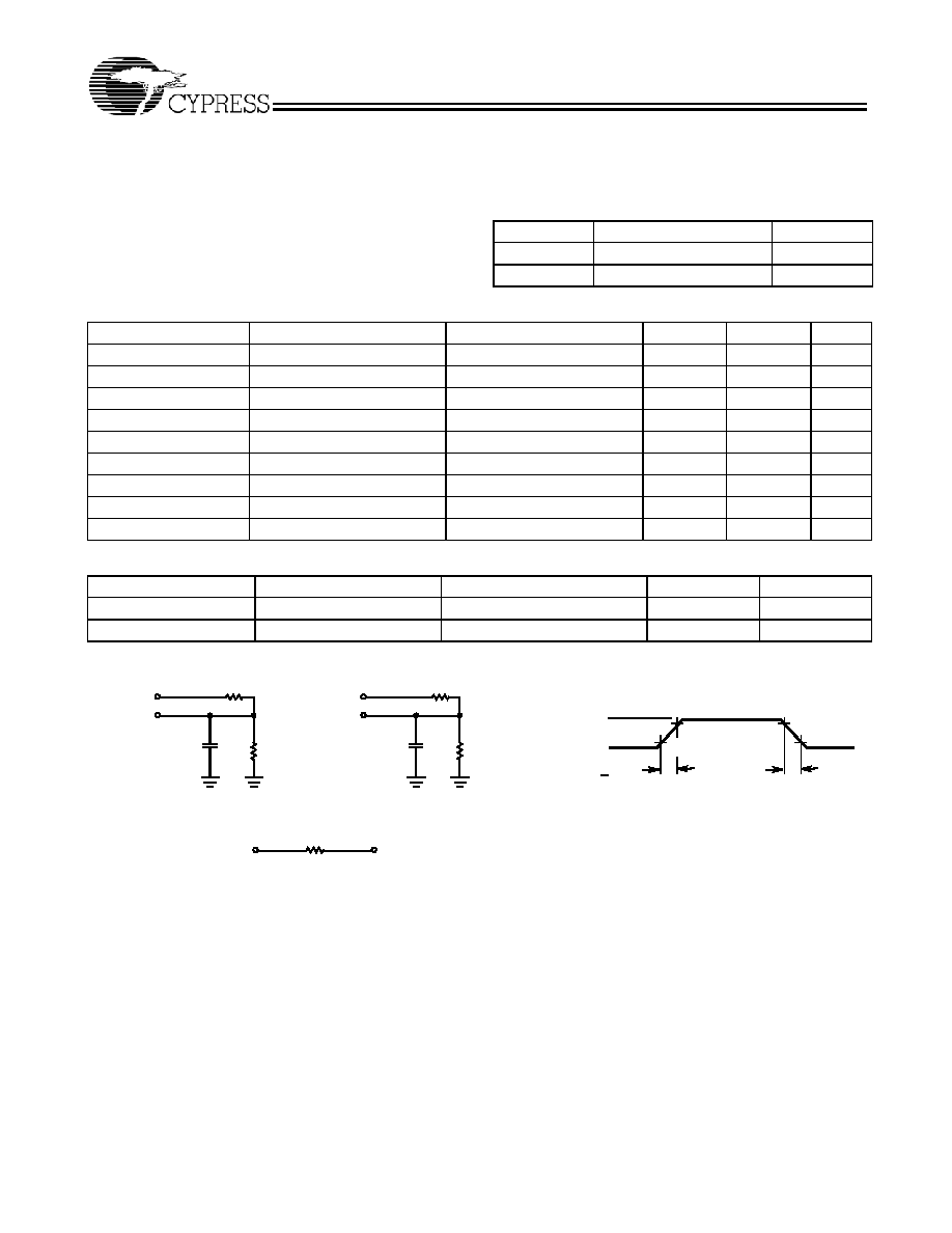
AC Test Loads and Waveforms
Notes:
1. Minimum DC input is –0.3V. During transactions, input may undershoot to –2.0V or overshoot to 7.0V for input currents less then 100 mA and periods shorter
than 20 ns.
2. The IOH parameter refers to high-level TTL output current; the IOL parameter refers to low-level TTL output current.
3. The Voltage on any input or I/O pin cannot exceed the power pin during power-up.
3.0V
5V
OUTPUT
R1 464
R2
250
50 pF
INCLUDING
JIG AND
SCOPE
GND
90%
10%
90%
10%
< 6ns
<6 ns
5V
OUTPUT
R1 464
R2
250
(a)
(b)
OUTPUT
1.75V
Equivalent to:
THVENIN EQUIVALENT (commercial/military)
ALL INPUT PULSES
tR
tF
5pF
163
相关PDF资料 |
PDF描述 |
|---|---|
| CY7C341B-35RC | UV PLD, 55 ns, CPGA84 |
| CY7C341B-35RI | UV PLD, 55 ns, CPGA84 |
| CY7C341B-25HC | UV PLD, 40 ns, CQCC84 |
| CY7C341B-25HI | UV PLD, 40 ns, CQCC84 |
| CY7C341B-35HC | UV PLD, 55 ns, CQCC84 |
相关代理商/技术参数 |
参数描述 |
|---|---|
| CY7C341B-35JI | 制造商:Cypress Semiconductor 功能描述:CPLD MAX 制造商:QP Semiconductor 功能描述:7C341B CYP DIE 35NS-PLCC |
| CY7C341B-35RI | 制造商:Cypress Semiconductor 功能描述:CPLD MAX? Family 3.75K Gates 192 Macro Cells 33.3MHz 0.65um Technology 5V 84-Pin Windowed PGA |
| CY7C342-25HC | 制造商:Cypress Semiconductor 功能描述:CMOS EPLD SMD 7C342 PLCC68 5V |
| CY7C342-30HC | 制造商:Cypress Semiconductor 功能描述: 制造商:Cypress Semiconductor 功能描述:Complex Erasable Programmable Logic Device, 128 Cell, 30ns, 68 Pin, Ceramic, PLCC |
| CY7C34235HMB | 制造商:CYPRESS 功能描述:New |
发布紧急采购,3分钟左右您将得到回复。