- 您现在的位置:买卖IC网 > PDF目录17066 > DC178A (Linear Technology)BOARD SAR ADC LTC1418 PDF资料下载
参数资料
| 型号: | DC178A |
| 厂商: | Linear Technology |
| 文件页数: | 10/28页 |
| 文件大小: | 0K |
| 描述: | BOARD SAR ADC LTC1418 |
| 设计资源: | DC178A Design File DC178A Schematic |
| 标准包装: | 1 |
| ADC 的数量: | 1 |
| 位数: | 14 |
| 采样率(每秒): | 200k |
| 数据接口: | 串行,并联 |
| 输入范围: | ±2.048 V |
| 已用 IC / 零件: | LTC1418 |
| 已供物品: | 板 |
| 相关产品: | LTC1418IG#PBF-ND - IC A/D CONV 14BIT SRL&PAR 28SSOP LTC1418AIG#TRPBF-ND - IC A/D CONV 14BIT SRL&PAR 28SSOP LTC1418CG#TRPBF-ND - IC A/D CONV 14BIT SRL&PAR 28SSOP LTC1418ACG#TRPBF-ND - IC A/D CONV 14BIT SRL&PAR 28SSOP LTC1418IG#TRPBF-ND - IC A/D CONV 14BIT SRL&PAR 28SSOP LTC1418CN#PBF-ND - IC A/D CONV 14BIT SRL&PAR 28-DIP LTC1418IN#PBF-ND - IC A/D CONV 14BIT SRL&PAR 28-DIP LTC1418CG#PBF-ND - IC A/D CONV 14BIT SRL&PAR 28SSOP LTC1418ACG#PBF-ND - IC A/D CONV 14BIT SRL&PAR 28SSOP LTC1418AIG#PBF-ND - IC A/D CONV 14BIT SRL&PAR 28SSOP 更多... |
第1页第2页第3页第4页第5页第6页第7页第8页第9页当前第10页第11页第12页第13页第14页第15页第16页第17页第18页第19页第20页第21页第22页第23页第24页第25页第26页第27页第28页
18
LTC1418
APPLICATIONS INFORMATION
WU
U
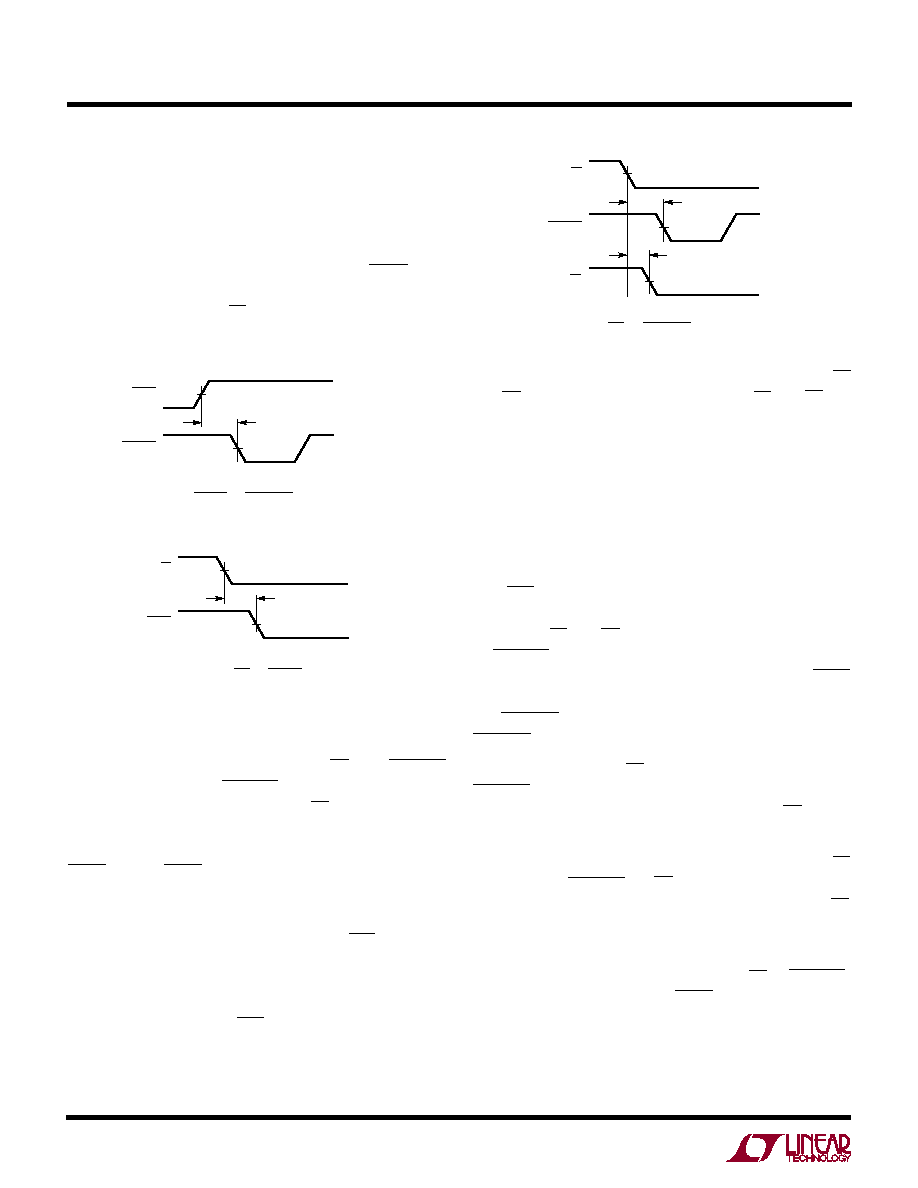
Figure 14. CS to CONVST Set-Up Timing
t2
t1
CS
CONVST
RD
1418 F14
mode is much slower since the reference circuit must
power up and settle to 0.005% for full 14-bit accuracy.
Sleep mode wake-up time is dependent on the value of
the capacitor connected to the REFCOMP (Pin 4). The
wake-up time is 30ms with the recommended 10
F
capacitor. Shutdown is controlled by Pin 22 (SHDN); the
ADC is in shutdown when it is low. The shutdown mode
is selected with Pin 25 (CS); low selects nap (see Figure
13b), high selects sleep.
t4
SHDN
CONVST
1418 F13a
Figure 13a. SHDN to CONVST Wake-Up Timing
t3
CS
SHDN
1418 F13b
Figure 13b. CS to SHDN Timing
Conversion Control
Conversion start is controlled by the CS and CONVST
inputs. A falling edge of CONVST pin will start a conversion
after the ADC has been selected (i.e., CS is low, see Figure
14). Once initiated, it cannot be restarted until the conver-
sion is complete. Converter status is indicated by the
BUSY output. BUSY is low during a conversion.
Data Output
The data format is controlled by the SER/PAR input pin;
logic low selects parallel output format. In parallel mode
the 14-bit data output word D0 to D13 is updated at the end
of each conversion on Pins 6 to 13 and Pins 15 to 20. A
logic high applied to SER/PAR selects the serial formatted
data output and Pins 16 to 20 assume their serial function,
Pins 6 to 13 and 15 are in the Hi-Z state. In either parallel
or serial data formats, outputs will be active only when CS
and RD are low. Any other combination of CS and RD will
three-state the output. In unipolar mode (VSS = 0V) the
data will be in straight binary format (corresponding to the
unipolar input range). In bipolar mode (VSS = –5V), the
data will be in two’s complement format (corresponding to
the bipolar input range).
Parallel Output Mode
Parallel mode is selected with a logic 0 applied to the
SER/PAR pin. Figures 15 through 19 show different modes
of parallel output operation. In modes 1a and 1b (Figures
15 and 16) CS and RD are both tied low. The falling edge
of CONVST starts the conversion. The data outputs are
always enabled and data can be latched with the BUSY
rising edge. Mode 1a shows operation with a narrow logic
low CONVST pulse. Mode 1b shows a narrow logic high
CONVST pulse.
In mode 2 (Figure 17) CS is tied low. The falling edge of
CONVST signal again starts the conversion. Data outputs
are in three-state until read by the MPU with the RD signal.
Mode 2 can be used for operation with a shared databus.
In slow memory and ROM modes (Figures 18 and 19), CS
is tied low and CONVST and RD are tied together. The MPU
starts the conversion and reads the output with the RD
signal. Conversions are started by the MPU or DSP (no
external sample clock).
In slow memory mode the processor takes RD (= CONVST)
low and starts the conversion. BUSY goes low forcing the
processor into a wait state. The previous conversion result
appears on the data outputs. When the conversion is
complete, the new conversion results appear on the data
相关PDF资料 |
PDF描述 |
|---|---|
| EBM22DSEN-S243 | CONN EDGECARD 44POS .156 EYELET |
| DC1186A | BOARD SAR ADC LTC2308 |
| MDP-XOMAP3630-10-1024512R | KIT MOBILE DEV ZOOM OMAP36X |
| V24C48E150BL3 | CONVERTER MOD DC/DC 48V 150W |
| EVAL-AD5764REBZ | EVAL BOARD FOR AD5764 |
相关代理商/技术参数 |
参数描述 |
|---|---|
| DC1792 | 功能描述:BOARD DAC LTC2756 RoHS:是 类别:编程器,开发系统 >> 评估板 - 数模转换器 (DAC) 系列:QuikEval™, SoftSpan™ 产品培训模块:Lead (SnPb) Finish for COTS Obsolescence Mitigation Program 标准包装:1 系列:- DAC 的数量:4 位数:12 采样率(每秒):- 数据接口:串行,SPI? 设置时间:3µs DAC 型:电流/电压 工作温度:-40°C ~ 85°C 已供物品:板 已用 IC / 零件:MAX5581 |
| DC1792A | 制造商:Linear Technology 功能描述:EVAL BOARD, LTC2756 18BIT DAC 制造商:Linear Technology 功能描述:EVAL BOARD, LTC2756 18BIT DAC; Silicon Manufacturer:Linear Technology; Silicon Core Number:LTC2756; Kit Contents:Evaluation Board for LTC2756; Features:SoftSpan IOUT DAC, SPI Interface; Length:29mm |
| DC1796A-A | 制造商:Linear Technology 功能描述:16BIT ADC Eval Brd 制造商:Linear Technology 功能描述:16BIT ADC Eval Brd; Silicon Manufacturer:Linear Technology; Silicon Core Number:LTC6360; Kit Application Type:Data Converter; Application Sub Type:ADC; Kit Contents:Board, Guide |
| DC1796A-B | 制造商:Linear Technology 功能描述:16BIT ADC Eval Brd 制造商:Linear Technology 功能描述:16BIT ADC Eval Brd; Silicon Manufacturer:Linear Technology; Silicon Core Number:LTC6360; Kit Application Type:Data Converter; Application Sub Type:ADC; Kit Contents:Board, Guide |
| DC1796A-C | 制造商:Linear Technology 功能描述:16BIT ADC Eval Brd 制造商:Linear Technology 功能描述:16BIT ADC Eval Brd; Silicon Manufacturer:Linear Technology; Silicon Core Number:LTC6360; Kit Application Type:Data Converter; Application Sub Type:ADC; Kit Contents:Board, Guide |
发布紧急采购,3分钟左右您将得到回复。