- 您现在的位置:买卖IC网 > PDF目录17061 > DC571A (Linear Technology)BOARD DELTA SIGMA ADC LTC2418 PDF资料下载
参数资料
| 型号: | DC571A |
| 厂商: | Linear Technology |
| 文件页数: | 21/48页 |
| 文件大小: | 0K |
| 描述: | BOARD DELTA SIGMA ADC LTC2418 |
| 软件下载: | QuikEval System |
| 设计资源: | DC571A Design File DC571A Schematic |
| 标准包装: | 1 |
| 系列: | QuikEval™ |
| ADC 的数量: | 1 |
| 位数: | 24 |
| 采样率(每秒): | 7.5 |
| 数据接口: | MICROWIRE?,串行,SPI? |
| 工作温度: | 0°C ~ 70°C |
| 已用 IC / 零件: | LTC2418 |
| 已供物品: | 板 |
| 相关产品: | DC590B-ND - BOARD DEMO USB SERIAL CONTROLLER LTC2418IGN#PBF-ND - IC ADC 24BIT DIFF INPUT 28SSOP LTC2418CGN#TRPBF-ND - IC ADC 24BIT DIFF INPUT 28SSOP LTC2418IGN#TRPBF-ND - IC ADC 24BIT DIFF INPUT 28SSOP LTC2418CGN#PBF-ND - IC ADC 24BIT DIFF INPUT 28SSOP LTC2418CGN-ND - IC ADC 24BIT DIFF INPUT 28SSOP LTC2418IGNTR-ND - IC ADC 24BIT DIFF INPUT 28SSOP LTC2418IGN-ND - IC ADC 24BIT DIFF INPUT 28SSOP LTC2418CGNTR-ND - IC ADC 24BIT DIFF INPUT 28SSOP |
第1页第2页第3页第4页第5页第6页第7页第8页第9页第10页第11页第12页第13页第14页第15页第16页第17页第18页第19页第20页当前第21页第22页第23页第24页第25页第26页第27页第28页第29页第30页第31页第32页第33页第34页第35页第36页第37页第38页第39页第40页第41页第42页第43页第44页第45页第46页第47页第48页
LTC2414/LTC2418
28
241418fa
RSOURCE ()
0 100 200 300 400 500 600 700 800 900 1000
+FS
ERROR
(ppm
OF
V
REF
)
2414/18 F15
300
240
180
120
60
0
VCC = 5V
REF+ = 5V
REF – = GND
IN+ = 3.75V
IN– = 1.25V
FO = GND
TA = 25°C
CIN = 0.01F
CIN = 0.1F
CIN = 1F, 10F
RSOURCE ()
0 100 200 300 400 500 600 700 800 900 1000
–
FS
ERROR
(ppm
OF
V
REF
)
2414/18 F16
0
–60
–120
–180
–240
–300
VCC = 5V
REF+ = 5V
REF – = GND
IN+ = 1.25V
IN– = 3.75V
FO = GND
TA = 25°C
CIN = 0.01F
CIN = 0.1F
CIN = 1F, 10F
VINCM (V)
0
0.5
1
1.5
2
2.5
3
3.5
4
4.5
5
OFFSET
ERROR
(ppm
OF
V
REF
)
2414/18 F17
120
100
80
60
40
20
0
–20
–40
–60
–80
–100
–120
FO = GND
TA = 25°C
RSOURCEIN– = 500
CIN = 10F
VCC = 5V
REF+ = 5V
REF – = GND
IN+ = IN– = VINCM
A:
RIN = +400
B:
RIN = +200
C:
RIN = +100
D:
RIN = 0
E:
RIN = –100
F:
RIN = –200
G:
RIN = –400
A
B
C
D
E
F
G
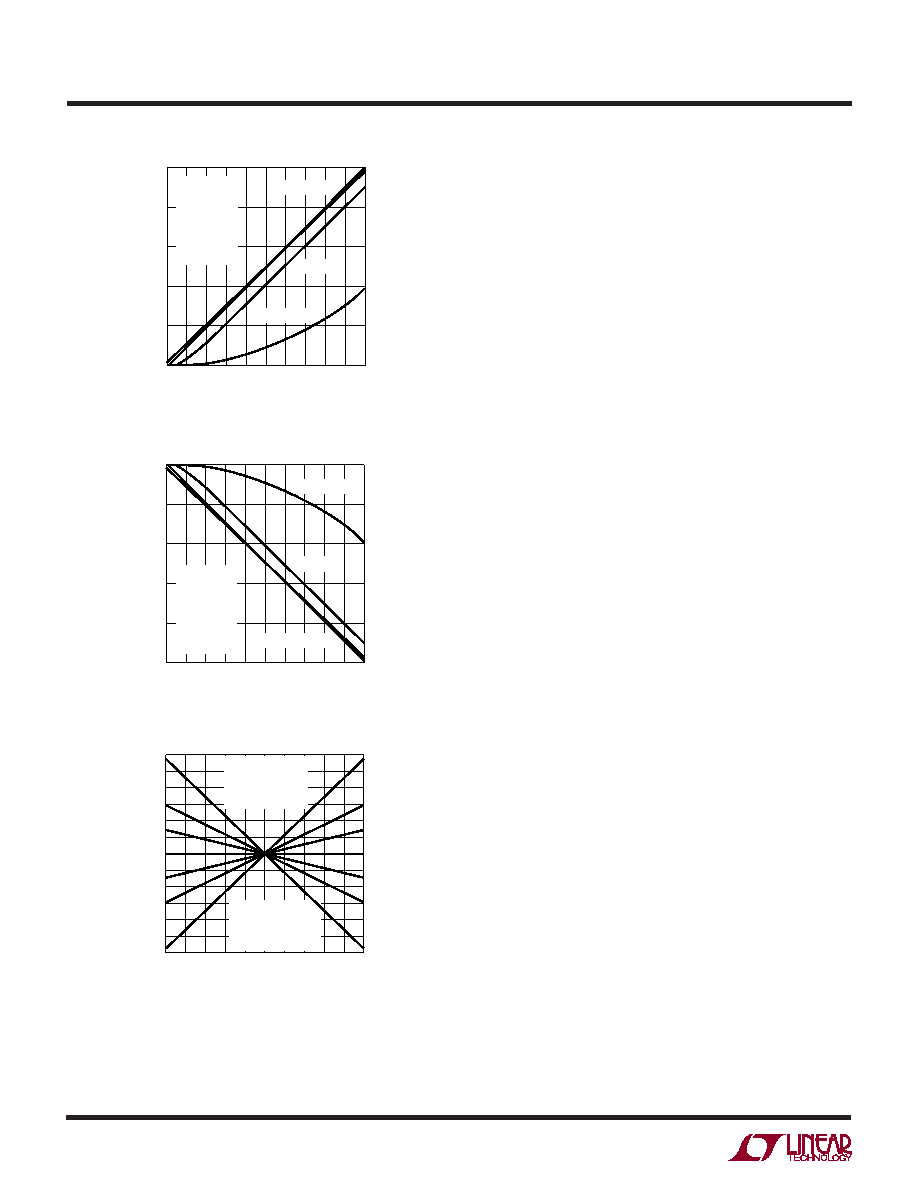
Figure 15. +FS Error vs RSOURCE at IN+ or IN– (Large CIN)
Figure 16. –FS Error vs RSOURCE at IN
+ or IN– (Large CIN)
Figure 17. Offset Error vs Common Mode Voltage
(VINCM = IN+ = IN–) and Input Source Resistance Imbalance
(
RIN = RSOURCEIN+ – RSOURCEIN–) for Large CIN Values (CIN ≥ 1F)
APPLICATIO S I FOR ATIO
WU
UU
1.78 10–6 fEOSCppm. Figure 17 shows the typical offset
error due to input common mode voltage for various
values of source resistance imbalance between the IN+
and IN– pins when large CIN values are used.
If possible, it is desirable to operate with the input signal
common mode voltage very close to the reference signal
common mode voltage as is the case in the ratiometric
measurement of a symmetric bridge. This configuration
eliminates the offset error caused by mismatched source
impedances.
The magnitude of the dynamic input current depends upon
the size of the very stable internal sampling capacitors and
upon the accuracy of the converter sampling clock. The
accuracy of the internal clock over the entire temperature
and power supply range is typical better than 0.5%. Such
a specification can also be easily achieved by an external
clock. When relatively stable resistors (50ppm/
°C) are
used for the external source impedance seen by IN+ and
IN–, the expected drift of the dynamic current, offset and
gain errors will be insignificant (about 1% of their respec-
tive values over the entire temperature and voltage range).
Even for the most stringent applications, a one-time
calibration operation may be sufficient.
In addition to the input sampling charge, the input ESD
protection diodes have a temperature dependent leakage
current. This current, nominally 1nA (
±10nA max), results
in a small offset shift. A 100
source resistance will create
a 0.1
V typical and 1V maximum offset voltage.
Reference Current
In a similar fashion, the LTC2414/LTC2418 samples the
differential reference pins REF+ and REF– transferring
small amount of charge to and from the external driving
circuits thus producing a dynamic reference current. This
current does not change the converter offset, but it may
degrade the gain and INL performance. The effect of this
current can be analyzed in the same two distinct situa-
tions.
For relatively small values of the external reference capaci-
tors (CREF < 0.01F), the voltage on the sampling capacitor
settles almost completely and relatively large values for
the source impedance result in only small errors. Such
相关PDF资料 |
PDF描述 |
|---|---|
| MIC2015-1.2YM6 TR | IC DISTRIBUTION SW 1.2A SOT23-6 |
| DC570A | BOARD DELTA SIGMA ADC LTC2440 |
| DC1012A-A | BOARD DELTA SIGMA ADC LTC2499 |
| DC1010A-A | BOARD DELTA SIGMA ADC LTC2493 |
| RCM15DCAH-S189 | CONN EDGECARD 30POS R/A .156 SLD |
相关代理商/技术参数 |
参数描述 |
|---|---|
| DC57-28 | 功能描述:ANT BKHAUL 28DBI 5.7GHZ 30" NFEM RoHS:是 类别:RF/IF 和 RFID >> RF 天线 系列:* 标准包装:1 系列:* |
| DC572A | 制造商:Linear Technology 功能描述:EVAL BOARD, LTC1592 16BIT DAC 制造商:Linear Technology 功能描述:EVAL BOARD, LTC1592 16BIT DAC; Silicon Manufacturer:Linear Technology; Silicon Core Number:LTC1592; Kit Contents:Evaluation Board for LTC1592; Features:Serial SoftSpan IOUT DAC; Length:29mm |
| DC573A | 功能描述:BOARD DELTA SIGMA ADC LTC2400 RoHS:是 类别:编程器,开发系统 >> 评估板 - 模数转换器 (ADC) 系列:QuikEval™ 产品培训模块:Obsolescence Mitigation Program 标准包装:1 系列:- ADC 的数量:1 位数:12 采样率(每秒):94.4k 数据接口:USB 输入范围:±VREF/2 在以下条件下的电源(标准):- 工作温度:-40°C ~ 85°C 已用 IC / 零件:MAX11645 已供物品:板,软件 |
| DC575A | 功能描述:BOARD DELTA SIGMA ADC LTC2410 RoHS:是 类别:编程器,开发系统 >> 评估板 - 模数转换器 (ADC) 系列:QuikEval™ 产品培训模块:Obsolescence Mitigation Program 标准包装:1 系列:- ADC 的数量:1 位数:12 采样率(每秒):94.4k 数据接口:USB 输入范围:±VREF/2 在以下条件下的电源(标准):- 工作温度:-40°C ~ 85°C 已用 IC / 零件:MAX11645 已供物品:板,软件 |
| DC579A | 功能描述:BOARD DAC LTC2600 RoHS:是 类别:编程器,开发系统 >> 评估板 - 数模转换器 (DAC) 系列:QuikEval™ 产品培训模块:Lead (SnPb) Finish for COTS Obsolescence Mitigation Program 标准包装:1 系列:- DAC 的数量:4 位数:12 采样率(每秒):- 数据接口:串行,SPI? 设置时间:3µs DAC 型:电流/电压 工作温度:-40°C ~ 85°C 已供物品:板 已用 IC / 零件:MAX5581 |
发布紧急采购,3分钟左右您将得到回复。