- 您现在的位置:买卖IC网 > PDF目录1994 > DS1689SN+T&R (Maxim Integrated Products)IC RTC SER NV RAM CTRL IN 28SOIC PDF资料下载
参数资料
| 型号: | DS1689SN+T&R |
| 厂商: | Maxim Integrated Products |
| 文件页数: | 35/36页 |
| 文件大小: | 0K |
| 描述: | IC RTC SER NV RAM CTRL IN 28SOIC |
| 标准包装: | 1,000 |
| 类型: | 时钟/日历 |
| 特点: | NVSRAM |
| 存储容量: | 114B |
| 时间格式: | HH:MM:SS(12/24 小时) |
| 数据格式: | YY-MM-DD-dd |
| 接口: | 并联 |
| 电源电压: | 2.7 V ~ 3.3 V,4.5 V ~ 5.5 V |
| 电压 - 电源,电池: | 2.5 V ~ 3.7 V |
| 工作温度: | -40°C ~ 85°C |
| 安装类型: | 表面贴装 |
| 封装/外壳: | 28-SOIC(0.295",7.50mm 宽) |
| 供应商设备封装: | 28-SOIC |
| 包装: | 带卷 (TR) |
第1页第2页第3页第4页第5页第6页第7页第8页第9页第10页第11页第12页第13页第14页第15页第16页第17页第18页第19页第20页第21页第22页第23页第24页第25页第26页第27页第28页第29页第30页第31页第32页第33页第34页当前第35页第36页
DS1689/DS1693
8 of 36
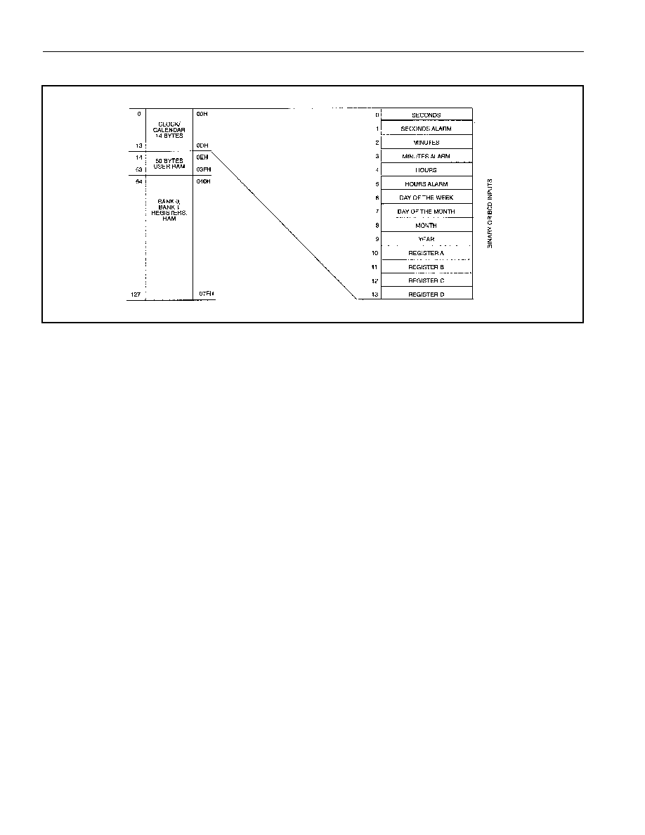
Figure 2. DS1689 Real-Time Clock Address Map
TIME, CALENDAR, AND ALARM LOCATIONS
The time and calendar information is obtained by reading the appropriate register bytes shown in Table 1.
The time, calendar, and alarm are set or initialized by writing the appropriate register bytes. The contents
of the time, calendar, and alarm registers can be either Binary or Binary-Coded Decimal (BCD) format.
Table 1 shows the binary and BCD formats of the twelve time, calendar, and alarm locations that reside in
both bank 0 and in bank 1, plus the two extended registers that reside in bank 1 only (bank 0 and bank 1
switching will be explained later in this text).
Before writing the internal time, calendar, and alarm registers, the SET bit in Register B should be written
to a logic 1 to prevent updates from occurring while access is being attempted. Also at this time, the data
format (binary or BCD) should be set via the data mode bit (DM) of Register B. All time, calendar, and
alarm registers must use the same data mode. The set bit in Register B should be cleared after the data
mode bit has been written to allow the real-time clock to update the time and calendar bytes.
Once initialized, the real-time clock makes all updates in the selected mode. The data mode cannot be
changed without reinitializing the 10 data bytes. The 24/12 bit cannot be changed without reinitializing
the hour locations. When the 12-hour format is selected, the high order bit of the hours byte represents
PM when it is a logic 1. The time, calendar, and alarm bytes are always accessible because they are
double-buffered. Once per second the 10 bytes are advanced by one second and checked for an alarm
condition. If a read of the time and calendar data occurs during an update, a problem exists where
seconds, minutes, hours, etc. may not correlate. The probability of reading incorrect time and calendar
data is low. Several methods of avoiding any possible incorrect time and calendar reads are covered later
in this text.
The four alarm bytes can be used in two ways. First, when the alarm time is written in the appropriate
hours, minutes, and seconds alarm locations, the alarm interrupt is initiated at the specified time each day
if the alarm enable bit is high. The second use condition is to insert a “don’t care” state in one or more of
the four alarm bytes. The “don’t care” code is any hexadecimal value from C0 to FF. The two most
significant bits of each byte set the “don’t care” condition when at logic 1. An alarm will be generated
each hour when the “don’t care” bits are set in the hours byte. Similarly, an alarm is generated every
相关PDF资料 |
PDF描述 |
|---|---|
| DS17285S-3NT | IC RTC 3V 2K NV RAM 24-SOIC |
| DS1742-100IND | IC RTC RAM Y2K 5V 100NS 24-EDIP |
| DS1743P-70+ | IC RTC RAM Y2K 5V 70NS 34-PCM |
| DS1744-70IND | IC RTC RAM Y2K 5V 70NS 28-EDIP |
| DS1746-70IND | IC RTC RAM Y2K 5V 70NS 32-EDIP |
相关代理商/技术参数 |
参数描述 |
|---|---|
| DS1689S-TRL | 功能描述:IC RTC SER W/NV RAM CTRL 28-SOIC RoHS:否 类别:集成电路 (IC) >> 时钟/计时 - 实时时钟 系列:- 产品培训模块:Obsolescence Mitigation Program 标准包装:1 系列:- 类型:时钟/日历 特点:警报器,闰年,SRAM 存储容量:- 时间格式:HH:MM:SS(12/24 小时) 数据格式:YY-MM-DD-dd 接口:SPI 电源电压:2 V ~ 5.5 V 电压 - 电源,电池:- 工作温度:-40°C ~ 85°C 安装类型:表面贴装 封装/外壳:8-WDFN 裸露焊盘 供应商设备封装:8-TDFN EP 包装:管件 |
| DS1691 | 功能描述:实时时钟 RoHS:否 制造商:Microchip Technology 功能:Clock, Calendar. Alarm RTC 总线接口:I2C 日期格式:DW:DM:M:Y 时间格式:HH:MM:SS RTC 存储容量:64 B 电源电压-最大:5.5 V 电源电压-最小:1.8 V 最大工作温度:+ 85 C 最小工作温度: 安装风格:Through Hole 封装 / 箱体:PDIP-8 封装:Tube |
| DS1691 WAF | 制造商:Texas Instruments 功能描述: |
| DS1691/1692 WAF | 制造商:Texas Instruments 功能描述: |
| DS1691A | 制造商:NSC 制造商全称:National Semiconductor 功能描述:(RS-422/RS-423) Line Drivers with TRI-STATE Outputs |
发布紧急采购,3分钟左右您将得到回复。