- 您现在的位置:买卖IC网 > PDF目录171225 > DS1862AB+ (MAXIM INTEGRATED PRODUCTS INC) SPECIALTY CONSUMER CIRCUIT, PBGA25 PDF资料下载
参数资料
| 型号: | DS1862AB+ |
| 厂商: | MAXIM INTEGRATED PRODUCTS INC |
| 元件分类: | 消费家电 |
| 英文描述: | SPECIALTY CONSUMER CIRCUIT, PBGA25 |
| 封装: | 5 X 5 MM, ROHS COMPLIANT, CSBGA-25 |
| 文件页数: | 1/42页 |
| 文件大小: | 586K |
| 代理商: | DS1862AB+ |
当前第1页第2页第3页第4页第5页第6页第7页第8页第9页第10页第11页第12页第13页第14页第15页第16页第17页第18页第19页第20页第21页第22页第23页第24页第25页第26页第27页第28页第29页第30页第31页第32页第33页第34页第35页第36页第37页第38页第39页第40页第41页第42页
DS1862A
XFP Laser Control and Digital Diagnostic IC
________________________________________________________________
Maxim Integrated Products
1
Rev 0; 10/08
For pricing, delivery, and ordering information, please contact Maxim Direct at 1-888-629-4642,
or visit Maxim’s website at www.maxim-ic.com.
General Description
The DS1862A is a closed-loop laser-driver control IC
with built-in digital diagnostics designed for XFP MSA.
The laser control function incorporates automatic power
control (APC) and allows extinction ratio control though
a temperature-indexed lookup table (LUT). The
DS1862A monitors up to seven analog inputs, including
temperature and monitor diode (MD) current, which are
used to regulate the laser bias current and extinction
ratio. Warning and alarm thresholds can be pro-
grammed to generate an interrupt if monitored signals
exceed tolerance. Calibration is also provided internally
using independent gain and offset scaling registers for
each of the monitored analog signals. Settings such as
programmed calibration data are stored in password-
protected EEPROM memory. Programming is accom-
plished through an I2C-compatible interface, which can
also be used to access diagnostic functionality.
Applications
Laser Control and Monitoring 10Gbps Optical
Transceiver Modules (XFP)
Laser Control and Monitoring
Digital Diagnostics in Optical Transmission
Features
Implements XFP MSA Requirements for Digital
Diagnostics, Serial ID, and User Memory
I2C-Compatible Serial Interface
Automatic Power Control (APC)
Extinction Ratio Control with Lookup Table
Seven Monitored Channels for Digital Diagnostics
(Five Basic Plus Two Auxiliary)
Internal Calibration of Monitored Channels
(Temp, VCC2/3, Bias Current, Transmitted, and
Received Power)
Programmable Quick-Trip Logic for Turning
Off Laser for Eye Safety
Access to Monitoring and ID Information
Programmable Alarm and Warning Thresholds
Operates from 3.3V or 5V Supply
25-Ball CSBGA, 5mm x 5mm Package
Internal or External Temperature Sensor
-40°C to +100°C Operating Temperature Range
One 8-Bit Buffered DAC
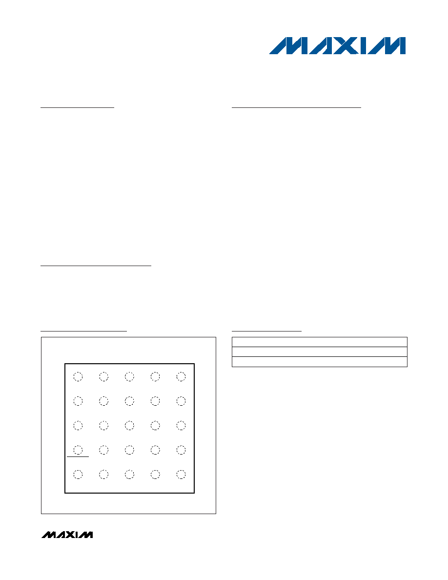
CSBGA (5mm x 5mm)
TOP VIEW
A
B
C
D
E
1
4
2
3
5
P-DOWN/
RST
SC-RX-LOS SC-RX-LOL
THRSET
RSSI
MODSET
SCL
RX-LOS
FETG
EN2
BIASSET
SDA
TX-D
EN1
AUX2MON
BMD
MOD-NR
INTERRUPT
AUX1MON
SC-TX-LOS
VCC3
MOD-DESEL
GND
IBIASMON
VCC2
+
Pin Configuration
+
Denotes a lead-free/RoHS-compliant package.
T&R = Tape and reel.
Ordering Information
Typical Operating Circuit appears at end of data sheet.
PART
TEMP RANGE
PIN-PACKAGE
DS1862AB+
-40°C to +100°C
25 CSBGA
DS1862AB+T&R
-40°C to +100°C
25 CSBGA
相关PDF资料 |
PDF描述 |
|---|---|
| DS1862AB+T&R | SPECIALTY CONSUMER CIRCUIT, PBGA25 |
| DS1868-100-IND | 100K DIGITAL POTENTIOMETER, 2-WIRE SERIAL CONTROL INTERFACE, 256 POSITIONS, PDIP14 |
| DS2-320-2AR | DIP20, IC SOCKET |
| DS1-314-1AR | DIP14, IC SOCKET |
| DS3-328-1AR | DIP28, IC SOCKET |
相关代理商/技术参数 |
参数描述 |
|---|---|
| DS1862AB+ | 功能描述:激光驱动器 XFP Laser Control & Digital Diagnostic RoHS:否 制造商:Micrel 数据速率:4.25 Gbps 工作电源电压:3 V to 3.6 V 电源电流:80 mA 最大工作温度:+ 85 C 封装 / 箱体:QFN-16 封装:Tube |
| DS1862AB+T&R | 制造商:Maxim Integrated Products 功能描述:XFP LASER CONTROL 25CSBGA - Tape and Reel 制造商:Maxim Integrated Products 功能描述:IC LASR CTRLR 7CHAN 5.5V 25CSBGA |
| DS1862AB+T&R | 功能描述:激光驱动器 XFP Laser Control & Digital Diagnostic RoHS:否 制造商:Micrel 数据速率:4.25 Gbps 工作电源电压:3 V to 3.6 V 电源电流:80 mA 最大工作温度:+ 85 C 封装 / 箱体:QFN-16 封装:Tube |
| DS1862AB+TR | 制造商:MAXIM 制造商全称:Maxim Integrated Products 功能描述:XFP Laser Control and Digital Diagnostic IC |
| DS1862B | 功能描述:激光驱动器 RoHS:否 制造商:Micrel 数据速率:4.25 Gbps 工作电源电压:3 V to 3.6 V 电源电流:80 mA 最大工作温度:+ 85 C 封装 / 箱体:QFN-16 封装:Tube |
发布紧急采购,3分钟左右您将得到回复。