参数资料
| 型号: | DS1874T+ |
| 厂商: | Maxim Integrated |
| 文件页数: | 26/88页 |
| 文件大小: | 0K |
| 描述: | IC CTLR SFP+ ANLG LDD 28-TQFN |
| 产品培训模块: | Lead (SnPb) Finish for COTS Obsolescence Mitigation Program |
| 标准包装: | 60 |
| 类型: | 激光二极管控制器 |
| 通道数: | 1 |
| 电源电压: | 2.85 V ~ 3.9 V |
| 电流 - 电源: | 2.5mA |
| 工作温度: | -40°C ~ 95°C |
| 封装/外壳: | 28-WFQFN 裸露焊盘 |
| 供应商设备封装: | 28-TQFN-EP(5x5) |
| 包装: | 管件 |
| 安装类型: | 表面贴装 |
| 其它名称: | 90-1874T+000 |
第1页第2页第3页第4页第5页第6页第7页第8页第9页第10页第11页第12页第13页第14页第15页第16页第17页第18页第19页第20页第21页第22页第23页第24页第25页当前第26页第27页第28页第29页第30页第31页第32页第33页第34页第35页第36页第37页第38页第39页第40页第41页第42页第43页第44页第45页第46页第47页第48页第49页第50页第51页第52页第53页第54页第55页第56页第57页第58页第59页第60页第61页第62页第63页第64页第65页第66页第67页第68页第69页第70页第71页第72页第73页第74页第75页第76页第77页第78页第79页第80页第81页第82页第83页第84页第85页第86页第87页第88页
�� ��
��
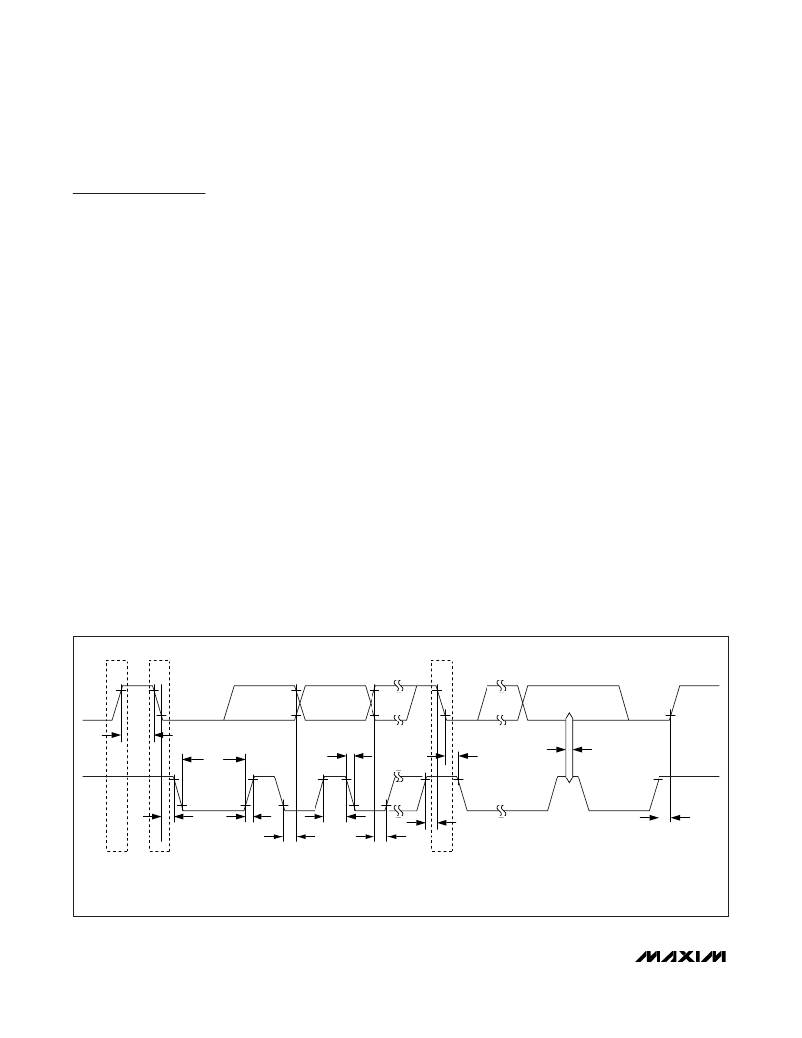
��SFP+� Controller� with� Digital� LDD� Interface�
�I2C� Communication�
�I� 2� C� Definitions�
�The� following� terminology� is� commonly� used� to�
�describe� I� 2� C� data� transfers.�
�Master� device:� The� master� device� controls� the�
�slave� devices� on� the� bus.� The� master� device� gen-�
�erates� SCL� clock� pulses� and� START� and� STOP�
�conditions.�
�Slave� devices:� Slave� devices� send� and� receive�
�data� at� the� master’s� request.�
�Bus� idle� or� not� busy:� Time� between� STOP� and�
�START� conditions� when� both� SDA� and� SCL� are� inac-�
�tive� and� in� their� logic-high� states.�
�START� condition:� A� START� condition� is� generated�
�by� the� master� to� initiate� a� new� data� transfer� with� a�
�slave.� Transitioning� SDA� from� high� to� low� while� SCL�
�remains� high� generates� a� START� condition.� See�
�Figure� 17� for� applicable� timing.�
�STOP� condition:� A� STOP� condition� is� generated� by�
�the� master� to� end� a� data� transfer� with� a� slave.�
�Transitioning� SDA� from� low� to� high� while� SCL�
�remains� high� generates� a� STOP� condition.� See�
�Figure� 17� for� applicable� timing.�
�Repeated� START� condition:� The� master� can� use� a�
�repeated� START� condition� at� the� end� of� one� data�
�transfer� to� indicate� that� it� will� immediately� initiate� a�
�new� data� transfer� following� the� current� one.�
�Repeated� STARTs� are� commonly� used� during� read�
�SDA�
�t� BUF�
�operations� to� identify� a� specific� memory� address� to�
�begin� a� data� transfer.� A� repeated� START� condition�
�is� issued� identically� to� a� normal� START� condition.�
�See� Figure� 17� for� applicable� timing.�
�Bit� write:� Transitions� of� SDA� must� occur� during� the�
�low� state� of� SCL.� The� data� on� SDA� must� remain� valid�
�and� unchanged� during� the� entire� high� pulse� of� SCL�
�plus� the� setup� and� hold� time� requirements� (Figure�
�17).� Data� is� shifted� into� the� device� during� the� rising�
�edge� of� the� SCL.�
�Bit� read:� At� the� end� a� write� operation,� the� master�
�must� release� the� SDA� bus� line� for� the� proper� amount�
�of� setup� time� (Figure� 17)� before� the� next� rising� edge�
�of� SCL� during� a� bit� read.� The� device� shifts� out� each�
�bit� of� data� on� SDA� at� the� falling� edge� of� the� previous�
�SCL� pulse� and� the� data� bit� is� valid� at� the� rising� edge�
�of� the� current� SCL� pulse.� Remember� that� the� master�
�generates� all� SCL� clock� pulses,� including� when� it� is�
�reading� bits� from� the� slave.�
�Acknowledgement� (ACK� and� NACK):� An� acknowl-�
�edgement� (ACK)� or� not� acknowledge� (NACK)� is�
�always� the� ninth� bit� transmitted� during� a� byte� trans-�
�fer.� The� device� receiving� data� (the� master� during� a�
�read� or� the� slave� during� a� write� operation)� performs�
�an� ACK� by� transmitting� a� zero� during� the� ninth� bit.� A�
�device� performs� a� NACK� by� transmitting� a� one� dur-�
�ing� the� 9th� bit.� Timing� (Figure� 17)� for� the� ACK� and�
�NACK� is� identical� to� all� other� bit� writes.� An� ACK� is�
�the� acknowledgment� that� the� device� is� properly�
�receiving� data.� A� NACK� is� used� to� terminate� a� read�
�t� LOW�
�t� F�
�t� HD:STA�
�t� SP�
�SCL�
�t� HD:STA�
�t� R�
�t� HIGH�
�t� SU:STA�
�t� SU:STO�
�t� HD:DAT�
�t� SU:DAT�
�STOP�
�START�
�REPEATED�
�START�
�NOTE:� TIMING� IS� REFERENCED� TO� V� IL(MAX)� AND� V� IH(MIN)� .�
�Figure� 17.� I� 2� C� Timing�
�26�
�______________________________________________________________________________________�
�相关PDF资料 |
PDF描述 |
|---|---|
| DS2129S+T&R | IC REGULATOR SCSI 16-SOIC |
| DS2438Z+T&R | IC MONITOR SMART BATTERY 8-SOIC |
| DS2703U+ | IC BATT AUTHENTICATE SHA-1 8UMAX |
| DS2705U+ | IC AUTHENTICATE SHA-1 8-UMAX |
| DS2710G+ | IC NIMH CHRGR SGL-CELL 10-TDFN |
相关代理商/技术参数 |
参数描述 |
|---|---|
| DS1874T+ | 功能描述:ADC / DAC多通道 SFP+ Controller w/ Dgtl LDD Interface RoHS:否 制造商:Texas Instruments 转换速率: 分辨率:8 bit 接口类型:SPI 电压参考: 电源电压-最大:3.6 V 电源电压-最小:2 V 最大工作温度:+ 85 C 安装风格:SMD/SMT 封装 / 箱体:VQFN-40 |
| DS1874T+T&R | 制造商:Maxim Integrated Products 功能描述:SFP+ CONTROLLER WITH DIGITAL LDD INTERFACE - Tape and Reel 制造商:Maxim Integrated Products 功能描述:MXMDS1874T+T&R SFP+ CTRLR FOR USE W/MAX3 制造商:Maxim Integrated Products 功能描述:IC CTLR SFP+ ANLG LDD 28-TQFN |
| DS1874T+T&R | 功能描述:ADC / DAC多通道 SFP+ Controller w/ Dgtl LDD Interface RoHS:否 制造商:Texas Instruments 转换速率: 分辨率:8 bit 接口类型:SPI 电压参考: 电源电压-最大:3.6 V 电源电压-最小:2 V 最大工作温度:+ 85 C 安装风格:SMD/SMT 封装 / 箱体:VQFN-40 |
| DS1874T+TR | 制造商:MAXIM 制造商全称:Maxim Integrated Products 功能描述:SFP+ Controller with Digital LDD Interface |
| DS1875 | 制造商:MAXIM 制造商全称:Maxim Integrated Products 功能描述:PON Triplexer and SFP Controller |
发布紧急采购,3分钟左右您将得到回复。