参数资料
| 型号: | DS1874T+ |
| 厂商: | Maxim Integrated |
| 文件页数: | 28/88页 |
| 文件大小: | 0K |
| 描述: | IC CTLR SFP+ ANLG LDD 28-TQFN |
| 产品培训模块: | Lead (SnPb) Finish for COTS Obsolescence Mitigation Program |
| 标准包装: | 60 |
| 类型: | 激光二极管控制器 |
| 通道数: | 1 |
| 电源电压: | 2.85 V ~ 3.9 V |
| 电流 - 电源: | 2.5mA |
| 工作温度: | -40°C ~ 95°C |
| 封装/外壳: | 28-WFQFN 裸露焊盘 |
| 供应商设备封装: | 28-TQFN-EP(5x5) |
| 包装: | 管件 |
| 安装类型: | 表面贴装 |
| 其它名称: | 90-1874T+000 |
第1页第2页第3页第4页第5页第6页第7页第8页第9页第10页第11页第12页第13页第14页第15页第16页第17页第18页第19页第20页第21页第22页第23页第24页第25页第26页第27页当前第28页第29页第30页第31页第32页第33页第34页第35页第36页第37页第38页第39页第40页第41页第42页第43页第44页第45页第46页第47页第48页第49页第50页第51页第52页第53页第54页第55页第56页第57页第58页第59页第60页第61页第62页第63页第64页第65页第66页第67页第68页第69页第70页第71页第72页第73页第74页第75页第76页第77页第78页第79页第80页第81页第82页第83页第84页第85页第86页第87页第88页
�� ��
��
��SFP+� Controller� with� Digital� LDD� Interface�
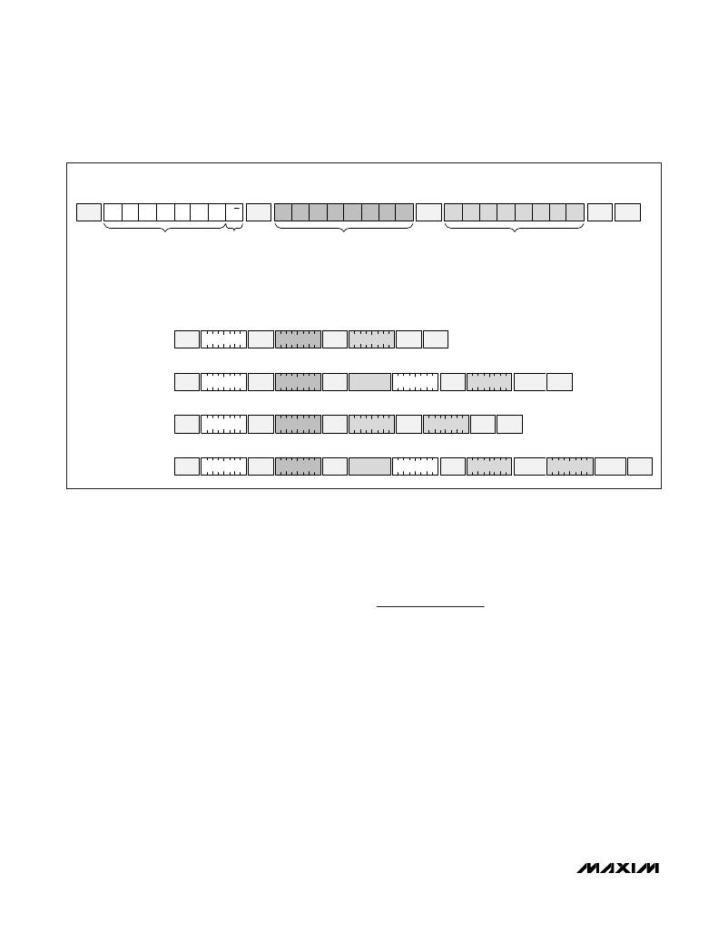
�TYPICAL� I� 2� C� WRITE� TRANSACTION�
�MSB�
�LSB�
�MSB�
�LSB�
�MSB�
�LSB�
�START�
�1�
�0�
�1�
�0�
�0�
�0�
�1�
�R/W�
�SLAVE�
�ACK�
�b7�
�b6�
�b5�
�b4�
�b3�
�b2�
�b1�
�b0�
�SLAVE�
�ACK�
�b7�
�b6�
�b5�
�b4�
�b3�
�b2�
�b1�
�b0�
�SLAVE�
�ACK�
�STOP�
�SLAVE�
�ADDRESS*�
�READ/�
�WRITE�
�REGISTER� ADDRESS�
�DATA�
�*IF� ASEL� IS� 0,� THE� SLAVE� ADDRESS� IS� A0h� FOR� THE� AUXILIARY� MEMORY� AND� A2h� FOR� THE� MAIN� MEMORY.�
�IF� ASEL� =� 1,� THE� SLAVE� ADDRESS� IS� DETERMINED� BY� TABLE� 02h,� REGISTER� 8Ch� FOR� THE� MAIN� MEMORY.� THE� AUXILIARY� MEMORY� CONTINUES� TO� BE� ADDRESSED� AT� A0h,� EXCEPT� WHEN� THE� PROGRAMMED�
�ADDRESS� FOR� THE� MAIN� MEMORY� IS� A0h.�
�EXAMPLE� I� 2� C� TRANSACTIONS� WITH� A2h� AS� THE� MAIN� MEMORY� DEVICE� ADDRESS�
�A2h�
�BAh�
�00h�
�A)� SINGLE-BYTE� WRITE�
�-WRITE� 00h� TO� REGISTER� BAh�
�START� 1� 0� 1� 0� 0� 0� 1� 0�
�SLAVE�
�ACK�
�10111010�
�SLAVE�
�ACK�
�00000000�
�SLAVE�
�ACK�
�STOP�
�A2h�
�BAh�
�A3h�
�DATA�
�START� 1� 0� 1� 0� 0� 0� 1� 0� SLAVE� 1� 0� 1� 1� 1� 0� 1� 0� SLAVE�
�1� 0� 1� 0� 0� 0� 1� 1� SLAVE�
�B)� SINGLE-BYTE� READ�
�-READ� REGISTER� BAh�
�ACK� ACK�
�REPEATED�
�START�
�ACK�
�DATA� IN� BAh�
�MASTER�
�NACK�
�STOP�
�C)� TWO-BYTE� WRITE�
�-WRITE� 01h� AND� 75h�
�TO� C8h� AND� C9h�
�A2h�
�START� 1� 0� 1� 0� 0� 0� 1� 0�
�SLAVE�
�ACK�
�C8h�
�11001000�
�SLAVE�
�ACK�
�01h�
�00000001�
�SLAVE�
�ACK�
�75h�
�01110101�
�SLAVE�
�ACK�
�STOP�
�A2h�
�C8h�
�A3h�
�DATA�
�DATA�
�D)� TWO-BYTE� READ�
�-READ� C8h� AND� C9h�
�START� 1� 0� 1� 0� 0� 0� 1� 0�
�SLAVE�
�ACK�
�11001000�
�SLAVE�
�ACK�
�REPEATED�
�START�
�10100011�
�SLAVE�
�ACK�
�DATA� IN� C8h�
�MASTER�
�ACK�
�DATA� IN� C9h�
�MASTER�
�NACK�
�STOP�
�Figure� 18.� Example� I� 2� C� Timing�
�cycle.� This� can� result� in� a� whole� page� being� worn� out�
�over� time� by� writing� a� single� byte� repeatedly.� Writing�
�a� page� one� byte� at� a� time� wears� the� EEPROM� out�
�eight� times� faster� than� writing� the� entire� page� at�
�once.� The� DS1874’s� EEPROM� write� cycles� are� speci-�
�fied� in� the� Nonvolatile� Memory� Characteristics� table.�
�The� specification� shown� is� at� the� worst-case� temper-�
�ature.� It� can� handle� approximately� ten� times� that�
�many� writes� at� room� temperature.� Writing� to� SRAM-�
�shadowed� EEPROM� memory� with� SEEB� =� 1� does� not�
�count� as� an� EEPROM� write� cycle� when� evaluating�
�the� EEPROM’s� estimated� lifetime.�
�Reading� a� single� byte� from� a� slave:� Unlike� the�
�write� operation� that� uses� the� memory� address� byte�
�to� define� where� the� data� is� to� be� written,� the� read�
�operation� occurs� at� the� present� value� of� the� memory�
�address� counter.� To� read� a� single� byte� from� the�
�slave,� the� master� generates� a� START� condition,�
�writes� the� slave� address� byte� with� R/� W� =� 1,� reads�
�the� data� byte� with� a� NACK� to� indicate� the� end� of� the�
�transfer,� and� generates� a� STOP� condition.�
�Manipulating� the� address� counter� for� reads:� A�
�dummy� write� cycle� can� be� used� to� force� the� address�
�pointer� to� a� particular� value.� To� do� this,� the� master�
�generates� a� START� condition,� writes� the� slave�
�address� byte� (R/� W� =� 0),� writes� the� memory� address�
�where� it� desires� to� read,� generates� a� repeated�
�START� condition,� writes� the� slave� address� byte� (R/� W�
�=� 1),� reads� data� with� ACK� or� NACK� as� applicable,�
�and� generates� a� STOP� condition.�
�Memory� Organization�
�The� DS1874� features� nine� separate� memory� tables� that�
�are� internally� organized� into� 8-byte� rows.�
�The� Lower� Memory� is� addressed� from� 00h� to� 7Fh� and�
�contains� alarm� and� warning� thresholds,� flags,� masks,�
�several� control� registers,� password� entry� area� (PWE),�
�and� the� table-select� byte.�
�Table� 01h� primarily� contains� user� EEPROM� (with� PW1�
�level� access)� as� well� as� alarm� and� warning-enable�
�bytes.�
�Table� 02h� is� a� multifunction� space� that� contains� config-�
�uration� registers,� scaling� and� offset� values,� passwords,�
�interrupt� registers� as� well� as� other� miscellaneous� con-�
�trol� bytes.�
�Table� 04h� contains� a� temperature-indexed� LUT� for�
�control� of� the� modulation� voltage.� The� modulation� LUT�
�can� be� programmed� in� 2°C� increments� over� the� -40°C�
�to� +102°C� range.�
�28�
�______________________________________________________________________________________�
�相关PDF资料 |
PDF描述 |
|---|---|
| DS2129S+T&R | IC REGULATOR SCSI 16-SOIC |
| DS2438Z+T&R | IC MONITOR SMART BATTERY 8-SOIC |
| DS2703U+ | IC BATT AUTHENTICATE SHA-1 8UMAX |
| DS2705U+ | IC AUTHENTICATE SHA-1 8-UMAX |
| DS2710G+ | IC NIMH CHRGR SGL-CELL 10-TDFN |
相关代理商/技术参数 |
参数描述 |
|---|---|
| DS1874T+ | 功能描述:ADC / DAC多通道 SFP+ Controller w/ Dgtl LDD Interface RoHS:否 制造商:Texas Instruments 转换速率: 分辨率:8 bit 接口类型:SPI 电压参考: 电源电压-最大:3.6 V 电源电压-最小:2 V 最大工作温度:+ 85 C 安装风格:SMD/SMT 封装 / 箱体:VQFN-40 |
| DS1874T+T&R | 制造商:Maxim Integrated Products 功能描述:SFP+ CONTROLLER WITH DIGITAL LDD INTERFACE - Tape and Reel 制造商:Maxim Integrated Products 功能描述:MXMDS1874T+T&R SFP+ CTRLR FOR USE W/MAX3 制造商:Maxim Integrated Products 功能描述:IC CTLR SFP+ ANLG LDD 28-TQFN |
| DS1874T+T&R | 功能描述:ADC / DAC多通道 SFP+ Controller w/ Dgtl LDD Interface RoHS:否 制造商:Texas Instruments 转换速率: 分辨率:8 bit 接口类型:SPI 电压参考: 电源电压-最大:3.6 V 电源电压-最小:2 V 最大工作温度:+ 85 C 安装风格:SMD/SMT 封装 / 箱体:VQFN-40 |
| DS1874T+TR | 制造商:MAXIM 制造商全称:Maxim Integrated Products 功能描述:SFP+ Controller with Digital LDD Interface |
| DS1875 | 制造商:MAXIM 制造商全称:Maxim Integrated Products 功能描述:PON Triplexer and SFP Controller |
发布紧急采购,3分钟左右您将得到回复。