- 您现在的位置:买卖IC网 > PDF目录97868 > DS2422X (DALLAS SEMICONDUCTOR) SPECIALTY MEMORY CIRCUIT, UUC PDF资料下载
参数资料
| 型号: | DS2422X |
| 厂商: | DALLAS SEMICONDUCTOR |
| 元件分类: | Memory IC:Other |
| 英文描述: | SPECIALTY MEMORY CIRCUIT, UUC |
| 文件页数: | 17/23页 |
| 文件大小: | 146K |
| 代理商: | DS2422X |
DS2422/DS2423
021998 3/23
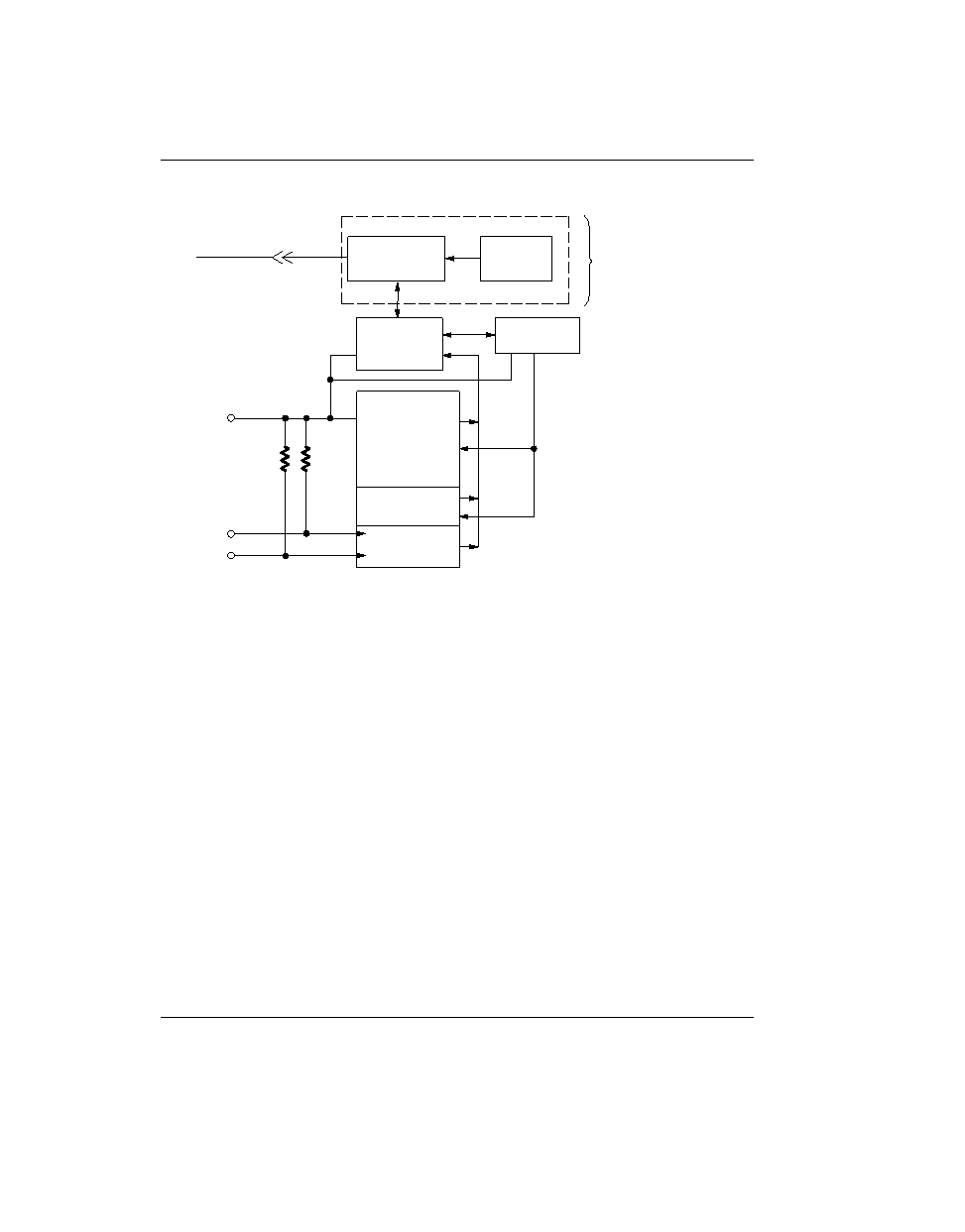
DS242X BLOCK DIAGRAM Figure 1
64-BIT
LASERED
ROM
1–WIRE
FUNCTION
CONTROL
MEMORY
FUNCTION
CONTROL
256–BIT
SCRATCHPAD
SRAM
4096–BIT
(DS2423)
1024–BIT
(DS2422)
(256–BIT PAGES)
DATA
1–WIRE BUS
PARASITE–POWERED
CIRCUITRY
PAGE
WRITE CYCLE
COUNTERS
EXTERNALLY
TRIGGERED
COUNTERS
RPI
Vbat
INPUT A
INPUT B
MEMORY
The memory map in Figure 5 shows a 32–byte page
called the scratchpad and additional 32–byte pages
called memory. The DS2422 contains pages 0 through
3 which make up the 1024–bit SRAM. The DS2423 con-
tains pages 0 through 15 which make up the 4096–bit
SRAM. The scratchpad is an additional page that acts
as a buffer when writing to memory.
ADDRESS REGISTERS AND TRANSFER
STATUS
Because of the serial data transfer, the DS242X
employs three address registers, called TA1, TA2 and
E/S (Figure 6). Registers TA1 and TA2 must be loaded
with the target address to which the data will be written
or from which data will be sent to the master upon a
Read command. Register E/S acts like a byte counter
and Transfer Status register. It is used to verify data
integrity with write commands. Therefore, the master
only has read access to this register. The lower five bits
of the E/S register indicate the address of the last byte
that has been written to the scratchpad. This address is
called Ending Offset. Bit 5 of the E/S register, called PF
or “partial byte flag,” is set if the number of data bits sent
by the master is not an integer multiple of 8. Bit 6 has no
function; it always reads 0. Note that the lowest five bits
of the target address also determine the address within
the scratchpad, where intermediate storage of data will
begin. This address is called byte offset. If the target
address (TA1) for a Write command is 03CH for exam-
ple, then the scratchpad will store incoming data begin-
ning at the byte offset 1CH and will be full after only four
bytes. The corresponding ending offset in this example
is 1FH. For best economy of speed and efficiency, the
target address for writing should point to the beginning
of a new page, i.e., the byte offset will be 0. Thus the full
32–byte capacity of the scratchpad is available, result-
ing also in the ending offset of 1FH. However, it is pos-
sible to write one or several contiguous bytes some-
where within a page. The ending offset together with the
Partial Flag support the master checking the data integ-
rity after a Write command. The highest valued bit of the
E/S register, called AA or Authorization Accepted, acts
as a flag to indicate that the data stored in the scratch-
pad has already been copied to the target memory
address. Writing data to the scratchpad clears this flag.
相关PDF资料 |
PDF描述 |
|---|---|
| DS2423P/T&R | SPECIALTY MEMORY CIRCUIT, PDSO6 |
| DS2423P | SPECIALTY MEMORY CIRCUIT, PDSO6 |
| DS2423X | SPECIALTY MEMORY CIRCUIT, UUC |
| DS2423 | 4K X 1 STANDARD SRAM, PDSO6 |
| DS2422 | 1K X 1 STANDARD SRAM, PDSO6 |
相关代理商/技术参数 |
参数描述 |
|---|---|
| DS2423 | 制造商:DALLAS 制造商全称:Dallas Semiconductor 功能描述:4kbit 1-Wire RAM with Counter |
| DS2423D/T&R | 制造商:Maxim Integrated Products 功能描述:IC SRAM 4KBIT 6FLIPCHIP |
| DS2423D/T&R | 功能描述:IC SRAM 4KBIT 6FCHIP RoHS:否 类别:集成电路 (IC) >> 存储器 系列:- 标准包装:150 系列:- 格式 - 存储器:EEPROMs - 串行 存储器类型:EEPROM 存储容量:4K (2 x 256 x 8) 速度:400kHz 接口:I²C,2 线串口 电源电压:2.5 V ~ 5.5 V 工作温度:-40°C ~ 85°C 封装/外壳:8-VFDFN 裸露焊盘 供应商设备封装:8-DFN(2x3) 包装:管件 产品目录页面:1445 (CN2011-ZH PDF) |
| DS2423MRAB0 | 制造商:Thomas & Betts 功能描述:300A,NLT,3P4W,MG,423,3P480V |
| DS2423P | 功能描述:静态随机存取存储器 RoHS:否 制造商:Cypress Semiconductor 存储容量:16 Mbit 组织:1 M x 16 访问时间:55 ns 电源电压-最大:3.6 V 电源电压-最小:2.2 V 最大工作电流:22 uA 最大工作温度:+ 85 C 最小工作温度:- 40 C 安装风格:SMD/SMT 封装 / 箱体:TSOP-48 封装:Tray |
发布紧急采购,3分钟左右您将得到回复。