- 您现在的位置:买卖IC网 > PDF目录1915 > DS26524GNA5+ (Maxim Integrated Products)IC TXRX T1/E1/J1 QUAD 256-CSBGA PDF资料下载
参数资料
| 型号: | DS26524GNA5+ |
| 厂商: | Maxim Integrated Products |
| 文件页数: | 101/273页 |
| 文件大小: | 0K |
| 描述: | IC TXRX T1/E1/J1 QUAD 256-CSBGA |
| 产品培训模块: | Lead (SnPb) Finish for COTS Obsolescence Mitigation Program |
| 标准包装: | 90 |
| 类型: | 线路接口装置(LIU) |
| 驱动器/接收器数: | 4/4 |
| 规程: | T1/E1/J1 |
| 电源电压: | 3.135 V ~ 3.465 V |
| 安装类型: | 表面贴装 |
| 封装/外壳: | 256-LBGA,CSBGA |
| 供应商设备封装: | 256-CSBGA(17x17) |
| 包装: | 托盘 |
第1页第2页第3页第4页第5页第6页第7页第8页第9页第10页第11页第12页第13页第14页第15页第16页第17页第18页第19页第20页第21页第22页第23页第24页第25页第26页第27页第28页第29页第30页第31页第32页第33页第34页第35页第36页第37页第38页第39页第40页第41页第42页第43页第44页第45页第46页第47页第48页第49页第50页第51页第52页第53页第54页第55页第56页第57页第58页第59页第60页第61页第62页第63页第64页第65页第66页第67页第68页第69页第70页第71页第72页第73页第74页第75页第76页第77页第78页第79页第80页第81页第82页第83页第84页第85页第86页第87页第88页第89页第90页第91页第92页第93页第94页第95页第96页第97页第98页第99页第100页当前第101页第102页第103页第104页第105页第106页第107页第108页第109页第110页第111页第112页第113页第114页第115页第116页第117页第118页第119页第120页第121页第122页第123页第124页第125页第126页第127页第128页第129页第130页第131页第132页第133页第134页第135页第136页第137页第138页第139页第140页第141页第142页第143页第144页第145页第146页第147页第148页第149页第150页第151页第152页第153页第154页第155页第156页第157页第158页第159页第160页第161页第162页第163页第164页第165页第166页第167页第168页第169页第170页第171页第172页第173页第174页第175页第176页第177页第178页第179页第180页第181页第182页第183页第184页第185页第186页第187页第188页第189页第190页第191页第192页第193页第194页第195页第196页第197页第198页第199页第200页第201页第202页第203页第204页第205页第206页第207页第208页第209页第210页第211页第212页第213页第214页第215页第216页第217页第218页第219页第220页第221页第222页第223页第224页第225页第226页第227页第228页第229页第230页第231页第232页第233页第234页第235页第236页第237页第238页第239页第240页第241页第242页第243页第244页第245页第246页第247页第248页第249页第250页第251页第252页第253页第254页第255页第256页第257页第258页第259页第260页第261页第262页第263页第264页第265页第266页第267页第268页第269页第270页第271页第272页第273页
DS26524 Quad T1/E1/J1 Transceiver
19 of 273
7.
PIN DESCRIPTIONS
7.1
Pin Functional Description
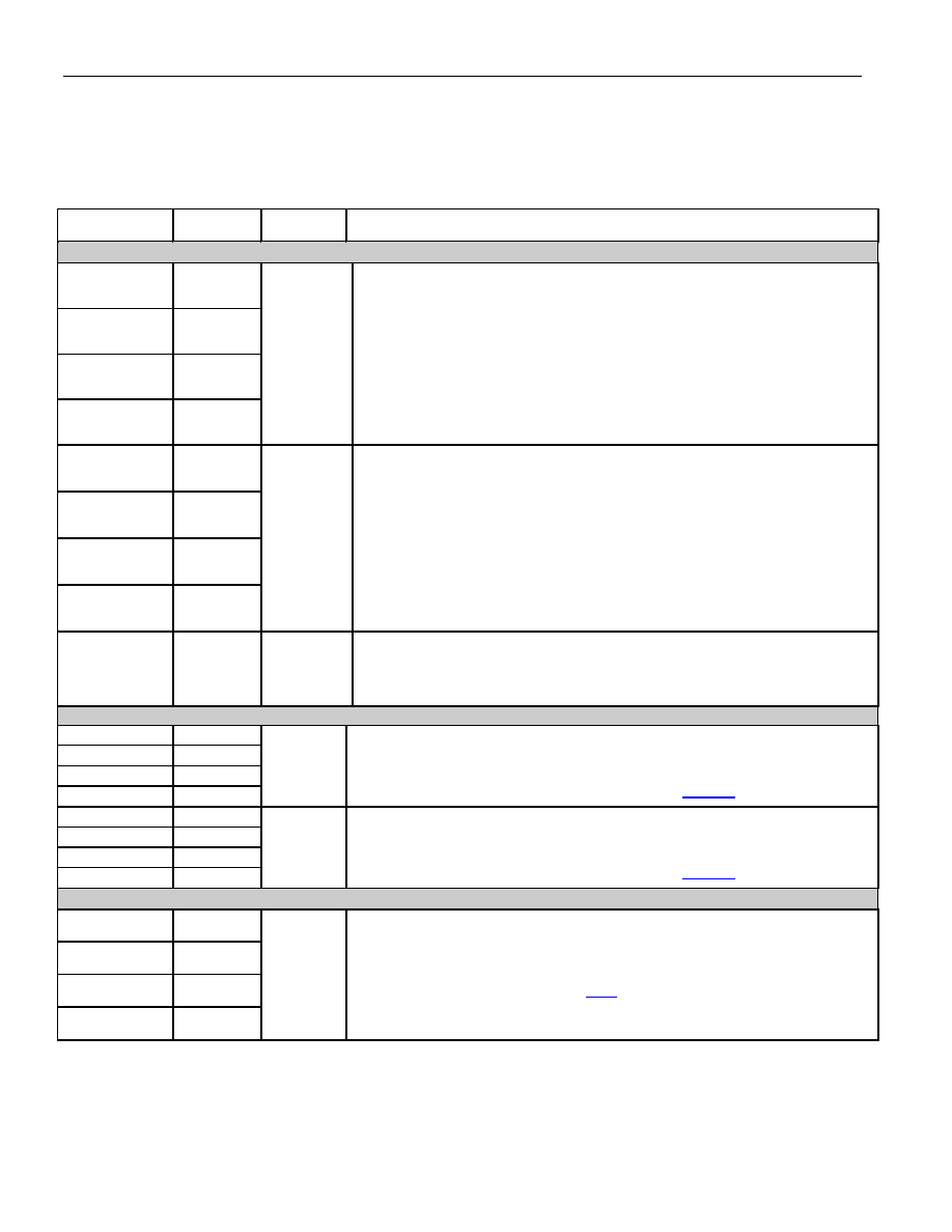
Table 7-1. Detailed Pin Descriptions
NAME
PIN
TYPE
FUNCTION
ANALOG TRANSMIT
TTIP1
A1, A2
TTIP2
H1, H2
TTIP3
J1 J2
TTIP4
T1, T2
Analog
Output,
High
Impedance
Transmit Bipolar Tip for Transceiver 1 to 4. These pins are differential line
driver tip outputs. These pins can be high impedance if:
If TXENABLE is low, the TTIP/TRING will be high impedance. Note that if
TXENABLE is low, the register settings for control of the TTIP/TRING are ignored
and output is high impedance.
The differential outputs of TTIPn and TRINGn can provide internal matched
impedance for E1 75
Ω , E1 120Ω, T1 100Ω, or J1 110Ω. The user has the option
of turning off internal termination.
Note: The two pins shown for each transmit bipolar tip (e.g., pins A1 and A2 for
TTIP1) should be tied together.
TRING1
A3, B3
TRING2
G3, H3
TRING3
J3, K3
TRING4
R3, T3
Analog
Output,
High
Impedance
Transmit Bipolar Ring for Transceiver 1 to 4. These pins are differential line
driver ring outputs. These pins can be high impedance if:
If TXENABLE is low, the TTIP/TRING will be high impedance. Note that if
TXENABLE is low, the register settings for control of the TTIP/TRING are ignored
and output is high impedance.
The differential outputs of TTIPn and TRINGn can provide internal matched
impedance for E1 75
Ω, E1 120Ω, T1 100Ω, or J1 110Ω. The user has the option
of turning off internal termination.
Note: The two pins shown for each transmit bipolar ring (e.g., pins A3 and B3 for
TRING1) should be tied together.
TXENABLE
L13
I
Transmit Enable. If this pin is pulled low, all transmitter outputs (TTIP and
TRING) are high impedance. The register settings for tri-state control of
TTIP/TRING are ignored if TXENABLE is low. If TXENABLE is high, the particular
driver can be tri-stated by the register settings.
ANALOG RECEIVE
RTIP1
C1
RTIP2
F1
RTIP3
L1
RTIP4
P1
Analog
Input
Receive Bipolar Tip for Transceiver 1 to 4. The differential inputs of RTIPn and
RRINGn can provide internal matched impedance for E1 75
Ω, E1 120Ω, T1 100Ω,
or J1 110
Ω. The user has the option of turning off internal termination via the LIU
Receive Impedance and Sensitivity Monitor register (LRISMR).
RRING1
C2
RRING2
F2
RRING3
L2
RRING4
P2
Analog
Input
Receive Bipolar Ring for Transceiver 1 to 4. The differential inputs of RTIPn and
RRINGn can provide internal matched impedance for E1 75
Ω, E1 120Ω, T1 100Ω,
or J1 110
Ω. The user has the option of turning off internal termination via the LIU
Receive Impedance and Sensitivity Monitor register (LRISMR).
TRANSMIT FRAMER
TSER1
F6
TSER2
E7
TSER3
R4
TSER4
N7
I
Transmit NRZ Serial Data. These pins are sampled on the falling edge of TCLK
when the transmit-side elastic store is disabled. These pins are sampled on the
falling edge of TSYSCLK when the transmit-side elastic store is enabled.
In IBO mode, data for multiple framers can be used in high-speed multiplexed
scheme. This is described in Section 8.8.2. The table there presents the
combination of framer data for each of the streams.
TSYSCLK is used as a reference when IBO is invoked.
相关PDF资料 |
PDF描述 |
|---|---|
| DS26528GNA5+ | IC TXRX T1/E1/J1 OCT 256-CSBGA |
| DS26900LN+ | IC JTAG MUX/SWITCH 144-LQFP |
| DS275E/T&R | IC TXRX LINE-PWR RS232 14-TSSOP |
| DS276S | IC TXRX LOW POWER RS-232 8-SOIC |
| DS2890P-000+T&R | IC POT DIGITAL 1-WIRE 100K 6TSOC |
相关代理商/技术参数 |
参数描述 |
|---|---|
| DS26524GNA5+ | 功能描述:网络控制器与处理器 IC 4-Port E1/T1/J1 Transceiver RoHS:否 制造商:Micrel 产品:Controller Area Network (CAN) 收发器数量: 数据速率: 电源电流(最大值):595 mA 最大工作温度:+ 85 C 安装风格:SMD/SMT 封装 / 箱体:PBGA-400 封装:Tray |
| DS26528 | 功能描述:网络控制器与处理器 IC 8-Port E1/T1/J1 Transceiver RoHS:否 制造商:Micrel 产品:Controller Area Network (CAN) 收发器数量: 数据速率: 电源电流(最大值):595 mA 最大工作温度:+ 85 C 安装风格:SMD/SMT 封装 / 箱体:PBGA-400 封装:Tray |
| DS26528_07 | 制造商:DALLAS 制造商全称:Dallas Semiconductor 功能描述:Octal T1/E1/J1 Transceiver |
| DS26528DK | 功能描述:网络开发工具 DS26528 Dev Kit RoHS:否 制造商:Rabbit Semiconductor 产品:Development Kits 类型:Ethernet to Wi-Fi Bridges 工具用于评估:RCM6600W 数据速率:20 Mbps, 40 Mbps 接口类型:802.11 b/g, Ethernet 工作电源电压:3.3 V |
| DS26528G | 功能描述:网络控制器与处理器 IC 8-Port E1/T1/J1 Transceiver RoHS:否 制造商:Micrel 产品:Controller Area Network (CAN) 收发器数量: 数据速率: 电源电流(最大值):595 mA 最大工作温度:+ 85 C 安装风格:SMD/SMT 封装 / 箱体:PBGA-400 封装:Tray |
发布紧急采购,3分钟左右您将得到回复。