- 您现在的位置:买卖IC网 > PDF目录4561 > DS3164N (Maxim Integrated Products)IC QUAD ATM/PACKET PHY 400-PBGA PDF资料下载
参数资料
| 型号: | DS3164N |
| 厂商: | Maxim Integrated Products |
| 文件页数: | 12/384页 |
| 文件大小: | 0K |
| 描述: | IC QUAD ATM/PACKET PHY 400-PBGA |
| 产品培训模块: | Lead (SnPb) Finish for COTS Obsolescence Mitigation Program |
| 标准包装: | 1 |
| 类型: | PHY 收发器 |
| 应用: | 测试设备 |
| 安装类型: | 表面贴装 |
| 封装/外壳: | 400-BBGA |
| 供应商设备封装: | 400-PBGA(27x27) |
| 包装: | 托盘 |
第1页第2页第3页第4页第5页第6页第7页第8页第9页第10页第11页当前第12页第13页第14页第15页第16页第17页第18页第19页第20页第21页第22页第23页第24页第25页第26页第27页第28页第29页第30页第31页第32页第33页第34页第35页第36页第37页第38页第39页第40页第41页第42页第43页第44页第45页第46页第47页第48页第49页第50页第51页第52页第53页第54页第55页第56页第57页第58页第59页第60页第61页第62页第63页第64页第65页第66页第67页第68页第69页第70页第71页第72页第73页第74页第75页第76页第77页第78页第79页第80页第81页第82页第83页第84页第85页第86页第87页第88页第89页第90页第91页第92页第93页第94页第95页第96页第97页第98页第99页第100页第101页第102页第103页第104页第105页第106页第107页第108页第109页第110页第111页第112页第113页第114页第115页第116页第117页第118页第119页第120页第121页第122页第123页第124页第125页第126页第127页第128页第129页第130页第131页第132页第133页第134页第135页第136页第137页第138页第139页第140页第141页第142页第143页第144页第145页第146页第147页第148页第149页第150页第151页第152页第153页第154页第155页第156页第157页第158页第159页第160页第161页第162页第163页第164页第165页第166页第167页第168页第169页第170页第171页第172页第173页第174页第175页第176页第177页第178页第179页第180页第181页第182页第183页第184页第185页第186页第187页第188页第189页第190页第191页第192页第193页第194页第195页第196页第197页第198页第199页第200页第201页第202页第203页第204页第205页第206页第207页第208页第209页第210页第211页第212页第213页第214页第215页第216页第217页第218页第219页第220页第221页第222页第223页第224页第225页第226页第227页第228页第229页第230页第231页第232页第233页第234页第235页第236页第237页第238页第239页第240页第241页第242页第243页第244页第245页第246页第247页第248页第249页第250页第251页第252页第253页第254页第255页第256页第257页第258页第259页第260页第261页第262页第263页第264页第265页第266页第267页第268页第269页第270页第271页第272页第273页第274页第275页第276页第277页第278页第279页第280页第281页第282页第283页第284页第285页第286页第287页第288页第289页第290页第291页第292页第293页第294页第295页第296页第297页第298页第299页第300页第301页第302页第303页第304页第305页第306页第307页第308页第309页第310页第311页第312页第313页第314页第315页第316页第317页第318页第319页第320页第321页第322页第323页第324页第325页第326页第327页第328页第329页第330页第331页第332页第333页第334页第335页第336页第337页第338页第339页第340页第341页第342页第343页第344页第345页第346页第347页第348页第349页第350页第351页第352页第353页第354页第355页第356页第357页第358页第359页第360页第361页第362页第363页第364页第365页第366页第367页第368页第369页第370页第371页第372页第373页第374页第375页第376页第377页第378页第379页第380页第381页第382页第383页第384页
DS3161/DS3162/DS3163/DS3164
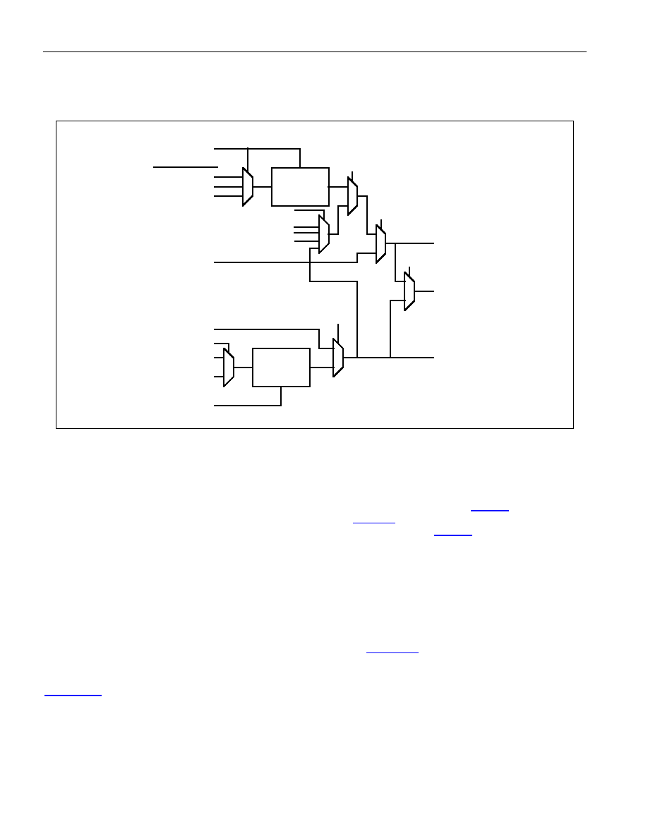
The 8 kHz reference logic tree is shown below.
Figure 10-6. 8KREF Logic
0
1
0
1
0
1
CLOCK DIVIDER
0
1
CLOCK DIVIDER
0
1
3
2
1
3
2
0
TX CLOCK
RX CLOCK
FRAME MODE
RX PLCP 8KREF
P8KRS[1]
P8KRS[0]
GPIO4
OTHER
PORT
8KREF
DS3 CLK
E3 CLK
STS-1 CLK
FROM CLAD
G8KRS[1:0]
G8KRS[2]
G8KIS
P8KREF
GLOBAL 8KREF
PORT 8KREF
TX PLCP 8KREF
10.4.3 One-Second Reference Generation
The one-second reference signal is used as an option to update the performance registers on a precise one
second interval. The generated internal signal should be about 50% duty cycle and it is derived from the Global 8
kHz reference signal by dividing it by 8000. The low to high edge on this signal will set the GL.SRL.ONESL latched
one second detect bit which can generate an interrupt when the GL.SRIE.ONESIE interrupt enable bit is set. The
low to high edge can also be used to generate performance monitor updates when GL.CR1.GPM[1:0]=1X.
10.4.4 General-Purpose I/O Pins
There are eight general-purpose I/O pins that can be used for general I/O, global signals and per port alarm
signals. Each pin is independently configurable to be a general-purpose input, general-purpose output, global
signal or port alarm. Two of the GPIO pins are assigned to each port and can be programmed to output one or two
alarm statuses using one or two GPIO pins. One of the two pins assigned to each port can be programmed as
global input or output signals. When the device is bonded out (or has ports powered down) to have 1, 2 or 3 ports
active, the GPIO pins associated with the disabled ports will still operate as either general-purpose inputs, general-
purpose outputs or global signals. When the ports are disabled and GL.GIOCR.GPIOx[1:0] = 01, the GPIO pin will
be an output driving low. The 8KREFI, TMEI, and PMU signals that can be sourced by the GPIO pin will be driven
low into the core logic when the GPIO pin is not selected for the source of the signal.
Table 10-12 lists the purpose and control thereof of the general-purpose I/O Pins.
相关PDF资料 |
PDF描述 |
|---|---|
| AMC22DRYN-S93 | CONN EDGECARD 44POS DIP .100 SLD |
| AMC22DRYH-S93 | CONN EDGECARD 44POS DIP .100 SLD |
| 24LC00-I/SN | IC EEPROM 128BIT 400KHZ 8SOIC |
| 24AA08T-I/MNY | IC EEPROM 8KBIT 400KHZ 8TDFN |
| HMC35DRYI-S13 | CONN EDGECARD 70POS .100 EXTEND |
相关代理商/技术参数 |
参数描述 |
|---|---|
| DS3166 | 制造商:Maxim Integrated Products 功能描述:6 PORT ATM/PHY 676-TEPBGA - Trays |
| DS3166N | 制造商:Maxim Integrated Products 功能描述:6 PORT ATM/PHY 676-TEPBGA IND - Trays |
| DS3168 | 制造商:Maxim Integrated Products 功能描述:8 PORT ATM/PHY 676-TEBGA - Trays |
| DS3168N | 制造商:Maxim Integrated Products 功能描述:8 PORT ATM/PHY 676-TEPBGA IND - Trays |
| DS316CC-F8 | 制造商:Enhance Technology 功能描述:ULTRASTOR DS SPARE PART: ONE (1) 6G SAS JBOD CONTROLLER KIT - Bulk |
发布紧急采购,3分钟左右您将得到回复。