参数资料
| 型号: | DS3911T+ |
| 厂商: | Maxim Integrated Products |
| 文件页数: | 24/24页 |
| 文件大小: | 0K |
| 描述: | IC DAC 10BIT I2C QUAD 14TDFN |
| 产品培训模块: | Lead (SnPb) Finish for COTS Obsolescence Mitigation Program |
| 标准包装: | 100 |
| 位数: | 10 |
| 数据接口: | I²C,串行 |
| 转换器数目: | 4 |
| 电压电源: | 单电源 |
| 功率耗散(最大): | 1.74W |
| 工作温度: | -40°C ~ 100°C |
| 安装类型: | 表面贴装 |
| 封装/外壳: | 14-WFDFN 裸露焊盘 |
| 供应商设备封装: | 14-TDFN-EP(3x5) |
| 包装: | 管件 |
| 输出数目和类型: | 4 电压,单极 |
| 采样率(每秒): | * |
DS3911
Temperature-Controlled, Nonvolatile,
I2C Quad DAC
9
Maxim Integrated
DAC Power-On Values
Each 10-bit DAC is controlled directly by the value in its
corresponding DAC VALUE register. Each DAC also has
a DAC POR register that contains the power-on-reset
(POR) value for the associated DAC, along with two con-
trol bits: enable (EN) and polarity (POL). See the Lower
Memory Register Descriptions section for complete lower
memory descriptions.
The DAC POR (DAC0 POR, DAC1 POR, DAC2 POR, and
DAC3 POR) registers are shadowed EEPROM with func-
tionality controlled by the shadow EEPROM bit (SEE). If
the SEE bit is high, the DAC POR registers function as
SRAM only. If the SEE bit is low, the registers are shad-
owed EEPROM and EEPROM write timing, tW, must be
observed.
On power-up, the initial DAC settings are always trans-
ferred from the DAC POR registers to the corresponding
DAC VALUE registers.
Manual Control Mode
On power-up, the device starts performing temperature
conversions and the DAC VALUE register whose corre-
sponding EN bit is set is updated by the LUT controller as
described in the Lookup Table Mode section. Clearing the
EN bit enables I2C writes to the corresponding DAC VALUE
and disables LUT controller updates. This allows the indi-
vidual DACs whose EN bit is cleared to be controlled by
writing the corresponding DAC VALUE register directly.
Lookup Table Mode
The device has four nonvolatile memory tables, one for each
of the four DACs. Each memory table is associated with an
individual DAC as follows: Table 04h (DAC0), Table 05h
(DAC1), Table 06h (DAC2), Table 07h (DAC3), and selected
by setting the table select bits, TS[3:0], in the CTRL regis-
ter. Each DAC memory table consists of a DAC LUT table
(addresses 80h–AFh) (DAC0 LUT, DAC1 LUT, DAC2 LUT,
and DAC3 LUT) and a DAC OFFSET table (addresses
F8h–FFh) (DAC0 OFFSET, DAC1 OFFSET, DAC2 OFFSET,
and DAC3 OFFSET). Because these four memory tables all
share the same address and register mapping, the TS[3:0]
bits must be used to select among them.
Each LUT address represents as little as a 2N change
in temperature. Table 1 shows the full temperature-to-
register mapping.
The first DAC OFFSET address corresponds to 32N of
temperature. After this, every 16N of temperature con-
verts into one DAC OFFSET address slot. Table 2 shows
the full temperature-to-register mapping.
The TINDEX register points to a LUT address slot. The
TINDEX register can operate in two modes, as defined
by the AEN bit. When the AEN bit is cleared, I2C writes
to the TINDEX register are enabled, and updates from
the LUT controller are blocked. The register can be used
to force DAC updates to be based on the user-selected
index. The TINDEX register directly addresses the LUT
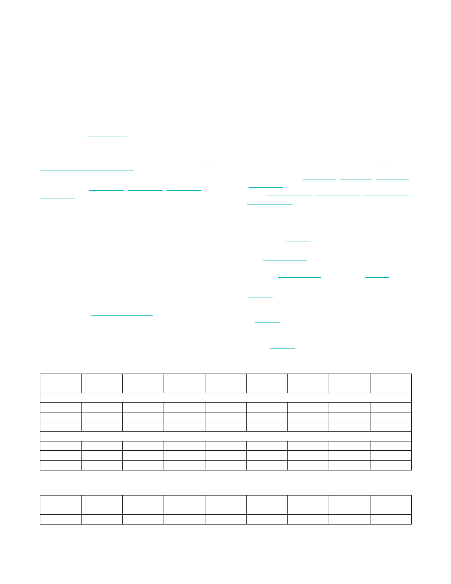
Table 1. LUT Temperature Mapping
Table 2. Offset Temperature Mapping
ROW
(HEX)
BYTE 0
BYTE 1
BYTE 2
BYTE 3
BYTE 4
BYTE 5
BYTE 6
BYTE 7
4NC LUT
80h
< -36N
-36N
-32N
-28N
-24N
-20N
-16N
-12N
88h
-8N
-4N
0N
+4N
+8N
+12N
+16N
+20N
90h
+24N
+28N
+32N
+36N
+40N
+44N
+48N
+52N
2NC LUT
98h
+56N
+58N
+60N
+62N
+64N
+66N
+68N
+70N
A0h
+72N
+74N
+76N
+78N
+80N
+82N
+84N
+86N
A8h
+88N
+90N
+92N
+94N
+96N
+98N
+100N
R
+102N
ROW
(HEX)
BYTE 0
BYTE 1
BYTE 2
BYTE 3
BYTE 4
BYTE 5
BYTE 6
BYTE 7
F8h
< -8N
-8N
+8N
+24N
+40N
+56N
+72N
R
+88N
相关PDF资料 |
PDF描述 |
|---|---|
| DS4000KI/WBGA | IC OSC TCXO 19.44MHZ 24-BGA |
| DS4026S+WCN | IC OSC TCXO 25MHZ 16-SOIC |
| DS4100HW+ | IC OSC CLOCK 100MHZ 10LCCC |
| DS4266P+ | IC OSC CLOCK 266MHZ 10-LCCC |
| DS4302Z-020/T&R | IC DAC 5-BIT SGL 0-2.0V 8-SOIC |
相关代理商/技术参数 |
参数描述 |
|---|---|
| DS3911T+ | 功能描述:ADC / DAC多通道 Fast APD Bias RoHS:否 制造商:Texas Instruments 转换速率: 分辨率:8 bit 接口类型:SPI 电压参考: 电源电压-最大:3.6 V 电源电压-最小:2 V 最大工作温度:+ 85 C 安装风格:SMD/SMT 封装 / 箱体:VQFN-40 |
| DS3911T+T | 功能描述:ADC / DAC多通道 Fast APD Bias RoHS:否 制造商:Texas Instruments 转换速率: 分辨率:8 bit 接口类型:SPI 电压参考: 电源电压-最大:3.6 V 电源电压-最小:2 V 最大工作温度:+ 85 C 安装风格:SMD/SMT 封装 / 箱体:VQFN-40 |
| DS3920 | 制造商:MAXIM 制造商全称:Maxim Integrated Products 功能描述:Fast Current Mirror |
| DS3920_1112 | 制造商:MAXIM 制造商全称:Maxim Integrated Products 功能描述:Fast Current Mirror |
| DS3920T-001+ | 功能描述:电流和电力监控器、调节器 Fast APD Bias RoHS:否 制造商:STMicroelectronics 产品:Current Regulators 电源电压-最大:48 V 电源电压-最小:5.5 V 工作温度范围:- 40 C to + 150 C 安装风格:SMD/SMT 封装 / 箱体:HPSO-8 封装:Reel |
发布紧急采购,3分钟左右您将得到回复。