参数资料
| 型号: | DS3911T+ |
| 厂商: | Maxim Integrated Products |
| 文件页数: | 3/24页 |
| 文件大小: | 0K |
| 描述: | IC DAC 10BIT I2C QUAD 14TDFN |
| 产品培训模块: | Lead (SnPb) Finish for COTS Obsolescence Mitigation Program |
| 标准包装: | 100 |
| 位数: | 10 |
| 数据接口: | I²C,串行 |
| 转换器数目: | 4 |
| 电压电源: | 单电源 |
| 功率耗散(最大): | 1.74W |
| 工作温度: | -40°C ~ 100°C |
| 安装类型: | 表面贴装 |
| 封装/外壳: | 14-WFDFN 裸露焊盘 |
| 供应商设备封装: | 14-TDFN-EP(3x5) |
| 包装: | 管件 |
| 输出数目和类型: | 4 电压,单极 |
| 采样率(每秒): | * |
DS3911
Temperature-Controlled, Nonvolatile,
I2C Quad DAC
11
Maxim Integrated
how a positive and negative tempco can be achieved by
adjusting DAC OFFSET values. The DACs are updated
after each temperature conversion.
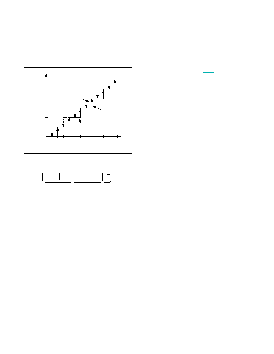
The LUT features 1NC hysteresis to prevent chatter-
ing if the measured temperature falls on the boundary
between two windows (Figure 5). This 1NC hysteresis is
implemented in the TINDEX register value calculation by
adding 1NC to temperature changes of negative slope.
Temperature Conversion and
Supply Voltage Monitoring
Temperature Conversion
The device features an internal 12-bit temperature sensor
that can drive the LUT and provide a measurement of the
ambient temperature over I2C by reading the value stored
in memory addresses 04h–05h. The sensor is functional
over the entire operating temperature range, and the results
are stored in signed two’s-complement format with a 1/16NC
resolution. See the Lower Memory, Register 04h–05h: TEMP
VALUE section for the temperature sensor’s bit weights. The
DONETEMP bit located in the CTRL register indicates
whether a temperature conversion has been completed
since the bit was last cleared.
Supply Voltage Monitoring
The device also features an internal 13-bit supply voltage
(VCC) monitor. A left-justified value of the supply voltage
measurement can be read over I2C at memory address-
es 06h–07h. To calculate the supply voltage, simply
convert the hexadecimal result into decimal and then
multiply it by the LSB as shown in the Analog Voltage
Monitoring Characteristics electrical specifications table.
The DONEVCC bit located in the CTRL register indicates
whether a VCC conversion has been completed since the
bit was last cleared.
Slave Address Byte and Address Pins
The slave address byte consists of a 7-bit slave address
plus a R/W bit, as shown in Figure 6. The device’s slave
address is determined by the state of the A0 and A1
address pins. These pins allow up to four devices to
reside on the same I2C bus. Address pins connected to
GND result in a 0 in the corresponding bit position in the
slave address. Conversely, address pins connected to
VCC result in a 1 in the corresponding bit positions. For
example, the device’s slave address byte is B0h when
A0 and A1 are grounded. See the I2C Serial Interface
section for more information.
I2C Serial Interface
I2C Definitions
The following terminology is commonly used to describe
the I2C AC Electrical Characteristics table for additional
information.
Master Device: The master device controls the slave
devices on the bus. The master device generates SCL
clock pulses and START and STOP conditions.
Slave Devices: Slave devices send and receive data
at the master’s request.
Bus Idle or Not Busy: Time between STOP and
START conditions when both SDA and SCL are inac-
tive and in their logic-high states.
START Condition: A START condition is generated by
the master to initiate a new data transfer with a slave.
Transitioning SDA from high to low while SCL remains
high generates a START condition.
Figure 5. LUT Hysteresis
Figure 6. DS3911 Slave Address Byte
MEMORY
LOCATION
9D
DECREASING
TEMPERATURE
INCREASING
TEMPERATURE
1°C HYSTERESIS
WINDOW
TEMPERATURE (°C)
56
58
60
62
64
66
9C
9B
9A
99
98
10
1
1R/W
A0
A1
0
MSB
LSB
SLAVE ADDRESS*
*THE SLAVE ADDRESS IS DETERMINED BY ADDRESS PINS A0 AND A1.
READ/WRITE BIT
相关PDF资料 |
PDF描述 |
|---|---|
| DS4000KI/WBGA | IC OSC TCXO 19.44MHZ 24-BGA |
| DS4026S+WCN | IC OSC TCXO 25MHZ 16-SOIC |
| DS4100HW+ | IC OSC CLOCK 100MHZ 10LCCC |
| DS4266P+ | IC OSC CLOCK 266MHZ 10-LCCC |
| DS4302Z-020/T&R | IC DAC 5-BIT SGL 0-2.0V 8-SOIC |
相关代理商/技术参数 |
参数描述 |
|---|---|
| DS3911T+ | 功能描述:ADC / DAC多通道 Fast APD Bias RoHS:否 制造商:Texas Instruments 转换速率: 分辨率:8 bit 接口类型:SPI 电压参考: 电源电压-最大:3.6 V 电源电压-最小:2 V 最大工作温度:+ 85 C 安装风格:SMD/SMT 封装 / 箱体:VQFN-40 |
| DS3911T+T | 功能描述:ADC / DAC多通道 Fast APD Bias RoHS:否 制造商:Texas Instruments 转换速率: 分辨率:8 bit 接口类型:SPI 电压参考: 电源电压-最大:3.6 V 电源电压-最小:2 V 最大工作温度:+ 85 C 安装风格:SMD/SMT 封装 / 箱体:VQFN-40 |
| DS3920 | 制造商:MAXIM 制造商全称:Maxim Integrated Products 功能描述:Fast Current Mirror |
| DS3920_1112 | 制造商:MAXIM 制造商全称:Maxim Integrated Products 功能描述:Fast Current Mirror |
| DS3920T-001+ | 功能描述:电流和电力监控器、调节器 Fast APD Bias RoHS:否 制造商:STMicroelectronics 产品:Current Regulators 电源电压-最大:48 V 电源电压-最小:5.5 V 工作温度范围:- 40 C to + 150 C 安装风格:SMD/SMT 封装 / 箱体:HPSO-8 封装:Reel |
发布紧急采购,3分钟左右您将得到回复。