参数资料
| 型号: | DS3911T+ |
| 厂商: | Maxim Integrated Products |
| 文件页数: | 5/24页 |
| 文件大小: | 0K |
| 描述: | IC DAC 10BIT I2C QUAD 14TDFN |
| 产品培训模块: | Lead (SnPb) Finish for COTS Obsolescence Mitigation Program |
| 标准包装: | 100 |
| 位数: | 10 |
| 数据接口: | I²C,串行 |
| 转换器数目: | 4 |
| 电压电源: | 单电源 |
| 功率耗散(最大): | 1.74W |
| 工作温度: | -40°C ~ 100°C |
| 安装类型: | 表面贴装 |
| 封装/外壳: | 14-WFDFN 裸露焊盘 |
| 供应商设备封装: | 14-TDFN-EP(3x5) |
| 包装: | 管件 |
| 输出数目和类型: | 4 电压,单极 |
| 采样率(每秒): | * |
DS3911
Temperature-Controlled, Nonvolatile,
I2C Quad DAC
13
Maxim Integrated
can be written at one time. If more than 8 bytes are
transmitted in the sequence, only the last 8 transmit-
ted bytes are stored. After the last physical memory
location in a particular page (8-byte page write), the
address counter automatically wraps back to the first
location in the same page for subsequent byte write
operations.
Acknowledge Polling: Any time a EEPROM byte is
written, the device requires the EEPROM write time
(tW) after the STOP condition to write the contents of
the byte to EEPROM. During the EEPROM write time,
the device does not acknowledge its slave address
because it is busy. It is possible to take advantage
of this phenomenon by repeatedly addressing the
device, which allows communication to continue as
soon as the device is ready. The alternative to acknowl-
edge polling is to wait for a maximum period of tW to
elapse before attempting to access the device.
Reading a Single Byte from a Slave: Unlike the write
operation that uses the specified memory address
byte to define where the data is to be written, the read
operation occurs at the present value of the memory
address counter. To read a single byte from the slave,
the master generates a START condition, writes the
slave address byte with R/W = 1, reads the data byte
with a NACK to indicate the end of the transfer, and
generates a STOP condition. However, since requiring
the master to keep track of the memory address coun-
ter is impractical, the next method should be used to
perform reads from a specified memory location.
Manipulating the Address Counter for Reads: A
dummy write cycle can be used to force the address
counter to a particular value. To do this, the master
generates a START condition, writes the slave address
byte (R/W = 0), writes the memory address where it
desires to read, generates a repeated START condi-
tion, writes the slave address byte (R/W = 1), reads
data with ACK or NACK as applicable, and generates
a STOP condition. Recall that the master must NACK
the last byte to inform the slave that no additional bytes
examples.
Reading Multiple Bytes from a Slave: The read
operation can be used to read multiple bytes with a
single transfer. When reading bytes from the slave,
the master simply ACKs the data byte if it desires to
read another byte before terminating the transaction.
After the master reads the last byte, it must NACK to
indicate the end of the transfer and generates a STOP
condition. During a single read sequence of multiple
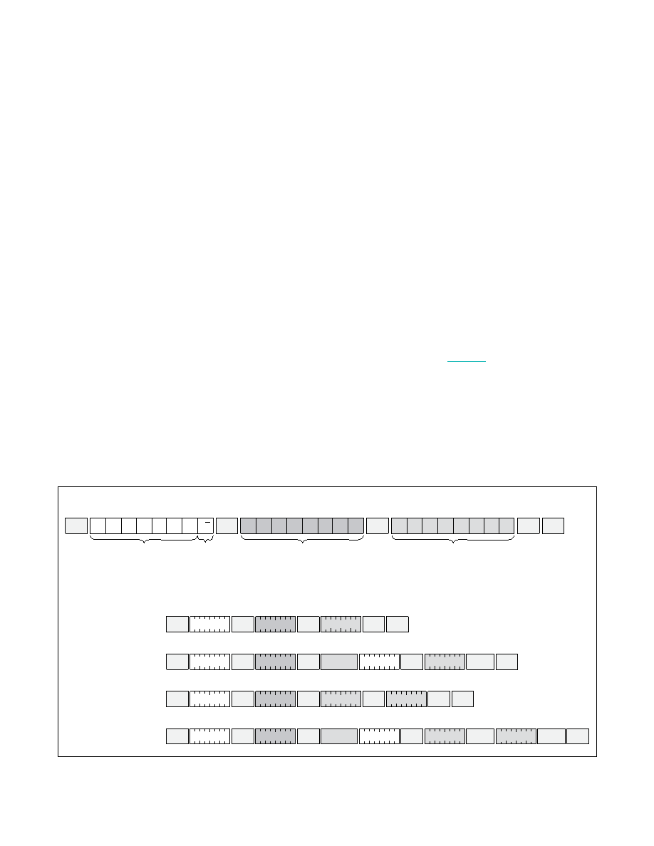
Figure 7. I2C Communication Examples
START
STOP
SLAVE
ACK
SLAVE
ACK
STOP
REPEATED
START
MASTER
NACK
1011000 0
B0h
00000000
00h
DATA
SLAVE
ACK
START
SLAVE
ACK
1011000 0
B0h
1 0110001
B1h
00000001
01h
SLAVE
ACK
SLAVE
ACK
STOP
DATA INTO 00h
STOP
SLAVE
ACK
STOP
DATA INTO 81h
DATA
START
SLAVE
ACK
1011000 0
B0h
10000000
80h
SLAVE
ACK
SLAVE
ACK
DATA INTO 80h
DATA
SLAVE
ACK
DATA IN 01h
DATA
REPEATED
START
MASTER
ACK
START
SLAVE
ACK
1011000 0
B0h
1 0110001
B1h
00000100
04h
SLAVE
ACK
SLAVE
ACK
DATA IN 04h
DATA
MASTER
NACK
DATA IN 05h
DATA
EXAMPLE I2C TRANSACTIONS WITH B0h AS THE DEVICE ADDRESS (WHEN A0 AND A1 ARE CONNECTED TO GND)
*THE SLAVE ADDRESS IS DETERMINED BY ADDRESS PINS A0 AND A1.
TYPICAL I2C WRITE TRANSACTION
SINGLE-BYTE WRITE
-WRITE CONTROL REGISTER (00h)
A)
2-BYTE WRITE
-WRITE LUT VALUES FOR REGISTERS
(80h81h)
C)
SINGLE-BYTE READ
-READ MODE REGISTER (01h)
B)
2-BYTE READ
-READ TEMPERATURE REGISTER
(04h05h)
D)
MSB
LSB
b7
b6
b5
b4
b3
b2
b1
b0
REGISTER ADDRESS
MSB
LSB
b7
b6
b5
b4
b3
b2
b1
b0
DATA
SLAVE
ACK
SLAVE
ACK
SLAVE
ADDRESS*
1
0
1
0
A1
A0
R/W
MSB
LSB
READ/
WRITE
相关PDF资料 |
PDF描述 |
|---|---|
| DS4000KI/WBGA | IC OSC TCXO 19.44MHZ 24-BGA |
| DS4026S+WCN | IC OSC TCXO 25MHZ 16-SOIC |
| DS4100HW+ | IC OSC CLOCK 100MHZ 10LCCC |
| DS4266P+ | IC OSC CLOCK 266MHZ 10-LCCC |
| DS4302Z-020/T&R | IC DAC 5-BIT SGL 0-2.0V 8-SOIC |
相关代理商/技术参数 |
参数描述 |
|---|---|
| DS3911T+ | 功能描述:ADC / DAC多通道 Fast APD Bias RoHS:否 制造商:Texas Instruments 转换速率: 分辨率:8 bit 接口类型:SPI 电压参考: 电源电压-最大:3.6 V 电源电压-最小:2 V 最大工作温度:+ 85 C 安装风格:SMD/SMT 封装 / 箱体:VQFN-40 |
| DS3911T+T | 功能描述:ADC / DAC多通道 Fast APD Bias RoHS:否 制造商:Texas Instruments 转换速率: 分辨率:8 bit 接口类型:SPI 电压参考: 电源电压-最大:3.6 V 电源电压-最小:2 V 最大工作温度:+ 85 C 安装风格:SMD/SMT 封装 / 箱体:VQFN-40 |
| DS3920 | 制造商:MAXIM 制造商全称:Maxim Integrated Products 功能描述:Fast Current Mirror |
| DS3920_1112 | 制造商:MAXIM 制造商全称:Maxim Integrated Products 功能描述:Fast Current Mirror |
| DS3920T-001+ | 功能描述:电流和电力监控器、调节器 Fast APD Bias RoHS:否 制造商:STMicroelectronics 产品:Current Regulators 电源电压-最大:48 V 电源电压-最小:5.5 V 工作温度范围:- 40 C to + 150 C 安装风格:SMD/SMT 封装 / 箱体:HPSO-8 封装:Reel |
发布紧急采购,3分钟左右您将得到回复。