- 您现在的位置:买卖IC网 > PDF目录10924 > DS4830T+T (Maxim Integrated Products)MCU 16B CTRL CALIBR MON 40-TQFN PDF资料下载
参数资料
| 型号: | DS4830T+T |
| 厂商: | Maxim Integrated Products |
| 文件页数: | 17/30页 |
| 文件大小: | 0K |
| 描述: | MCU 16B CTRL CALIBR MON 40-TQFN |
| 产品培训模块: | Lead (SnPb) Finish for COTS Obsolescence Mitigation Program |
| 标准包装: | 2,500 |
| 系列: | MAXQ® |
| 核心处理器: | RISC |
| 芯体尺寸: | 16-位 |
| 速度: | 10MHz |
| 连通性: | 3 线,I²C,SPI |
| 外围设备: | 欠压检测/复位,POR,PWM,WDT |
| 输入/输出数: | 31 |
| 程序存储器容量: | 64KB(32K x 16) |
| 程序存储器类型: | 闪存 |
| RAM 容量: | 1K x 16 |
| 电压 - 电源 (Vcc/Vdd): | 3 V ~ 3.6 V |
| 数据转换器: | A/D 18x13b,D/A 8x12b |
| 振荡器型: | 内部 |
| 工作温度: | -40°C ~ 85°C |
| 封装/外壳: | 16-WQFN 裸露焊盘 |
| 包装: | 带卷 (TR) |
| 其它名称: | 90-4830T+TRL |
第1页第2页第3页第4页第5页第6页第7页第8页第9页第10页第11页第12页第13页第14页第15页第16页当前第17页第18页第19页第20页第21页第22页第23页第24页第25页第26页第27页第28页第29页第30页
DS4830
Optical Microcontroller
24
Maxim Integrated
Analog-to-Digital Converter
and Sample/Hold
The analog-to-digital converter (ADC) controller is the
digital interface block between the CPU and the ADC. It
provides all the necessary controls to the ADC and the
CPU interface. The ADC uses a set of SFRs for configur-
ing the ADC in desired mode of operation.
The device contains a 13-bit ADC with an input mux
(Figure 9). The mux selects the ADC input from 16 single-
ended or eight differential inputs. Additionally, the chan-
nels can be configured to convert internal and external
temperature, VDD, internal reference, or REFINA/B. Two
channels can be programmed to be sample/hold inputs.
The internal channel is used exclusively to measure the
die temperature. The SFR registers control the ADC.
ADC
When used in voltage input mode, the voltage applied on
the corresponding channel (differential or single-ended)
is converted to a digital readout. The ADC can be set up
to continuously poll selected input channels (continuous-
sequence mode) or run a short burst of conversions
and enter a shutdown mode to conserve power (single-
sequence mode).
In voltage mode there are four full-scale values that can
be programmed. These values can be trimmed by modi-
fying the associated gain registers (ADCG1, ADCG2,
ADCG3, ADCG4). By default these are set to 1.2V, 0.6V,
2.4V, and 4.8V full scale.
The ADCCLK is derived from the system clock with divi-
sion ratio defined by the ADC control register. An A/D
conversion takes 15 ADCCLK cycles to complete with
additional four core clocks used for data processing.
Internally every channel is converted twice and the aver-
age of two conversions is written to the data buffer. This
gives each conversion result in (30 x ADC Clock Period
+ 800ns). ADC sampling rate is approximately 40ksps
for the fastest ADC clock (core clock/8). In applications
where extending the acquisition time is desired, the sam-
ple can be acquired over a prolonged period determined
by the ADC control register.
Each ADC channel can have its own configuration, such
as differential mode select, data alignment select, acqui-
sition extension enable, and ADC gain select, etc. The
ADC also has 24 (0 to 23) 16-bit data buffers for con-
version result storage. The ADC data available interrupt
flag (ADDAI) can be configured to trigger an interrupt
following a predetermined number of samples. Once set,
ADDAI can be cleared by software or at the start of a
conversion process.
Sample/Hold
Pin combinations GP2-GP3 and GP12-GP13 can be
used for sample/hold conversions if enabled in the SHCN
register. These two can be independently enabled or
disabled by writing a 1 or 0 to their corresponding bit
locations in SHCN register. A data buffer location is
reserved for each channel. When a particular channel is
enabled, a sample of the input voltage is taken when a
signal is issued on the SHEN pin, converted and stored
in the corresponding data buffer.
The two sample/hold channels can sample simultane-
ously on the same SHEN signal or different SHEN signals
depending on the SH_DUAL bit in the SHCN SFR.
The sample/hold data available interrupt flag (SHnDAI)
can be configured to trigger an interrupt following sam-
ple completion. Once set, SHnDAI can be cleared by
software.
Each sample/hold circuit consists of a sampling capaci-
tor, charge injection nulling switches, and a buffer.
Also included is a discharge circuit used to discharge
parasitic capacitance on the input node and the sample
capacitor before sampling begins. The negative input
pins can be used to reduce ground offsets and noise.
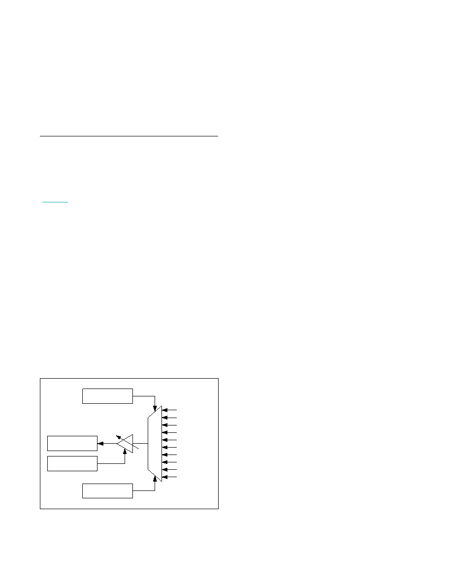
Figure 9. ADC Block Diagram
ADC-S[15:0]
ADC-D[7:0][P/N]
ADC-SHP[1:0]
ADC-SHN[1:0]
ADC-REFIN[A/B]
ADC-VDD
ADC-VREF_2.5V
ADC-TEXT_A(+/-)
ADC-TEXT_B(+/-)
ADC-TINT
MUX
ADCONV
(START CONVERSATION)
ADCCFG
PGA
ADGAIN
13-BIT ADC
相关PDF资料 |
PDF描述 |
|---|---|
| ISD5008PY | IC VOICE REC/PLAY 4-8MIN 28-DIP |
| VI-24H-CV-S | CONVERTER MOD DC/DC 52V 150W |
| 73S1209F-44IMR/F | IC SMART CARD READER 44-QFN |
| VE-B3Y-IV-F3 | CONVERTER MOD DC/DC 3.3V 99W |
| VI-243-CV-S | CONVERTER MOD DC/DC 24V 150W |
相关代理商/技术参数 |
参数描述 |
|---|---|
| DS485 | 制造商:NSC 制造商全称:National Semiconductor 功能描述:Low Power RS-485/RS-422 Multipoint Transceiver |
| DS485M | 功能描述:RS-422/RS-485 接口 IC RoHS:否 制造商:Maxim Integrated 数据速率:1136 Kbps 工作电源电压:3 V to 5.5 V 电源电流:5.9 mA 工作温度范围:- 40 C to + 85 C 安装风格:SMD/SMT 封装 / 箱体:SOIC-28 封装:Tube |
| DS485M | 制造商:Texas Instruments 功能描述:RS485/422 LOW POWER TRNSCVR SOIC8 |
| DS485M/NOPB | 功能描述:RS-422/RS-485 接口 IC RoHS:否 制造商:Maxim Integrated 数据速率:1136 Kbps 工作电源电压:3 V to 5.5 V 电源电流:5.9 mA 工作温度范围:- 40 C to + 85 C 安装风格:SMD/SMT 封装 / 箱体:SOIC-28 封装:Tube |
| DS485MX | 功能描述:RS-422/RS-485 接口 IC RoHS:否 制造商:Maxim Integrated 数据速率:1136 Kbps 工作电源电压:3 V to 5.5 V 电源电流:5.9 mA 工作温度范围:- 40 C to + 85 C 安装风格:SMD/SMT 封装 / 箱体:SOIC-28 封装:Tube |
发布紧急采购,3分钟左右您将得到回复。