- 您现在的位置:买卖IC网 > PDF目录19361 > DSP56321VF200 (Freescale Semiconductor)IC DSP 24BIT 200MHZ 196-BGA PDF资料下载
参数资料
| 型号: | DSP56321VF200 |
| 厂商: | Freescale Semiconductor |
| 文件页数: | 6/84页 |
| 文件大小: | 0K |
| 描述: | IC DSP 24BIT 200MHZ 196-BGA |
| 标准包装: | 126 |
| 系列: | DSP56K/Symphony |
| 类型: | 定点 |
| 接口: | 主机接口,SSI,SCI |
| 时钟速率: | 200MHz |
| 非易失内存: | ROM(576 B) |
| 芯片上RAM: | 576kB |
| 电压 - 输入/输出: | 3.30V |
| 电压 - 核心: | 1.60V |
| 工作温度: | -40°C ~ 100°C |
| 安装类型: | 表面贴装 |
| 封装/外壳: | 196-FBGA |
| 供应商设备封装: | 196-MAPBGA(15x15) |
| 包装: | 托盘 |
第1页第2页第3页第4页第5页当前第6页第7页第8页第9页第10页第11页第12页第13页第14页第15页第16页第17页第18页第19页第20页第21页第22页第23页第24页第25页第26页第27页第28页第29页第30页第31页第32页第33页第34页第35页第36页第37页第38页第39页第40页第41页第42页第43页第44页第45页第46页第47页第48页第49页第50页第51页第52页第53页第54页第55页第56页第57页第58页第59页第60页第61页第62页第63页第64页第65页第66页第67页第68页第69页第70页第71页第72页第73页第74页第75页第76页第77页第78页第79页第80页第81页第82页第83页第84页
DSP56321 Technical Data, Rev. 11
1-8
Freescale Semiconductor
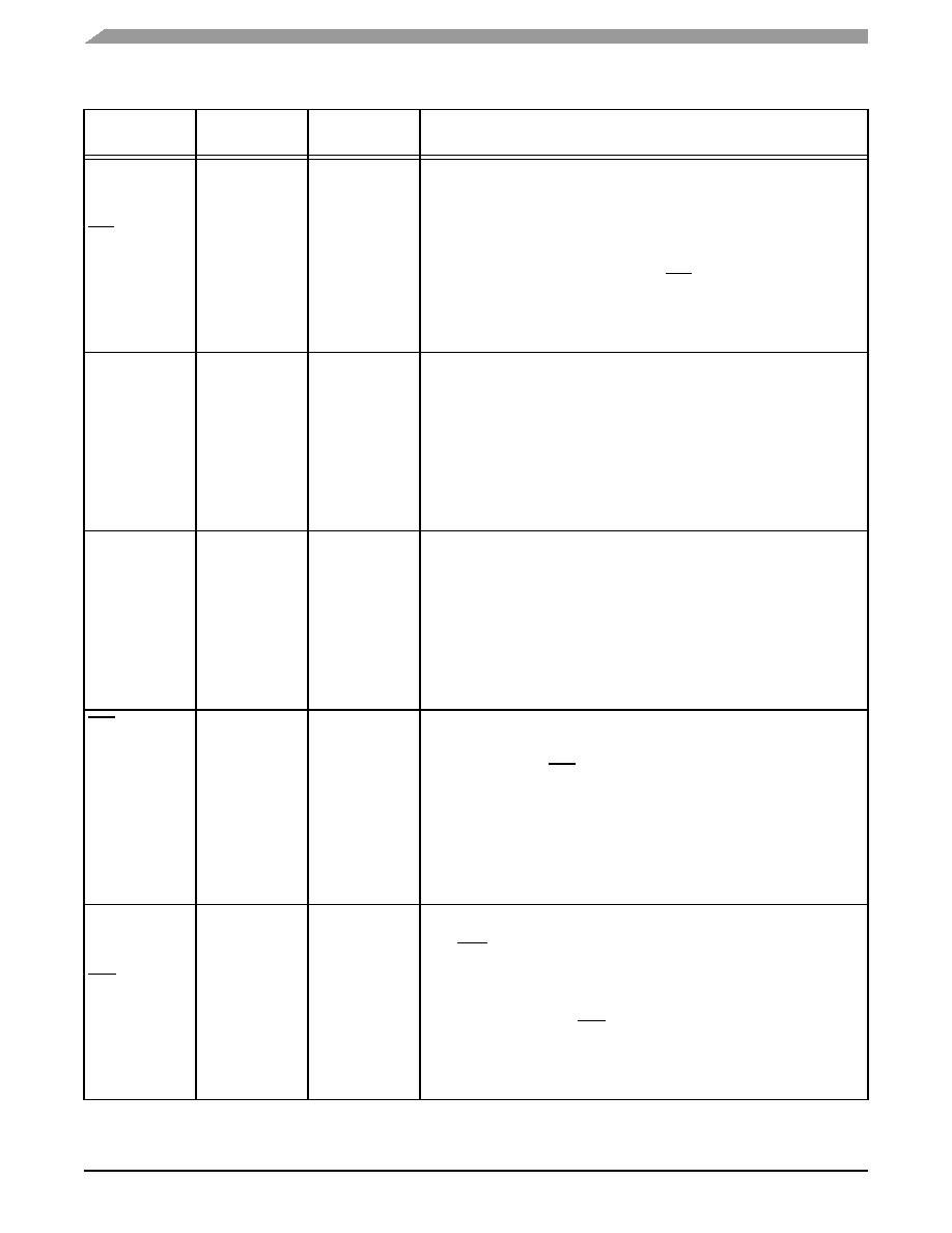
Signals/Connections
HA0
HAS/HAS
PB8
Input
Input or Output
Ignored Input
Host Address Input 0—When the HI08 is programmed to interface with a
nonmultiplexed host bus and the HI function is selected, this signal is line 0 of
the host address input bus.
Host Address Strobe—When the HI08 is programmed to interface with a
multiplexed host bus and the HI function is selected, this signal is the host
address strobe (HAS) Schmitt-trigger input. The polarity of the address strobe is
programmable but is configured active-low (HAS) following reset.
Port B 8—When the HI08 is configured as GPIO through the HI08 Port Control
Register, this signal is individually programmed as an input or output through the
HI08 Data Direction Register.
HA1
HA8
PB9
Input
Input or Output
Ignored Input
Host Address Input 1—When the HI08 is programmed to interface with a
nonmultiplexed host bus and the HI function is selected, this signal is line 1 of
the host address (HA1) input bus.
Host Address 8—When the HI08 is programmed to interface with a multiplexed
host bus and the HI function is selected, this signal is line 8 of the host address
(HA8) input bus.
Port B 9—When the HI08 is configured as GPIO through the HI08 Port Control
Register, this signal is individually programmed as an input or output through the
HI08 Data Direction Register.
HA2
HA9
PB10
Input
Input or Output
Ignored Input
Host Address Input 2—When the HI08 is programmed to interface with a
nonmultiplexed host bus and the HI function is selected, this signal is line 2 of
the host address (HA2) input bus.
Host Address 9—When the HI08 is programmed to interface with a multiplexed
host bus and the HI function is selected, this signal is line 9 of the host address
(HA9) input bus.
Port B 10—When the HI08 is configured as GPIO through the HI08 Port Control
Register, this signal is individually programmed as an input or output through the
HI08 Data Direction Register.
HCS/HCS
HA10
PB13
Input
Input or Output
Ignored Input
Host Chip Select—When the HI08 is programmed to interface with a
nonmultiplexed host bus and the HI function is selected, this signal is the host
chip select (HCS) input. The polarity of the chip select is programmable but is
configured active-low (HCS) after reset.
Host Address 10—When the HI08 is programmed to interface with a
multiplexed host bus and the HI function is selected, this signal is line 10 of the
host address (HA10) input bus.
Port B 13—When the HI08 is configured as GPIO through the HI08 Port Control
Register, this signal is individually programmed as an input or output through the
HI08 Data Direction Register.
HRW
HRD/HRD
PB11
Input
Input or Output
Ignored Input
Host Read/Write—When the HI08 is programmed to interface with a single-
data-strobe host bus and the HI function is selected, this signal is the Host
Read/Write (HRW) input.
Host Read Data—When the HI08 is programmed to interface with a double-
data-strobe host bus and the HI function is selected, this signal is the HRD
strobe Schmitt-trigger input. The polarity of the data strobe is programmable but
is configured as active-low (HRD) after reset.
Port B 11—When the HI08 is configured as GPIO through the HI08 Port Control
Register, this signal is individually programmed as an input or output through the
HI08 Data Direction Register.
Table 1-10.
Host Interface (Continued)
Signal Name
Type
State During
Reset1,2
Signal Description
相关PDF资料 |
PDF描述 |
|---|---|
| IRS2158DSPBF | IC DVR HALF BRIDGE 600V 16-SOIC |
| IRS2166DSPBF | IC PFC/BALLAST/HALF BRDG 16-SOIC |
| TPSC686M006R0150 | CAP TANT 68UF 6.3V 20% 2312 |
| RBM10DRKI | CONN EDGECARD 20POS DIP .156 SLD |
| EP1K30FC256-3 | IC ACEX 1K FPGA 30K 256-FBGA |
相关代理商/技术参数 |
参数描述 |
|---|---|
| DSP56321VF200R2 | 功能描述:数字信号处理器和控制器 - DSP, DSC 321 MAP 200MHZ T&R RoHS:否 制造商:Microchip Technology 核心:dsPIC 数据总线宽度:16 bit 程序存储器大小:16 KB 数据 RAM 大小:2 KB 最大时钟频率:40 MHz 可编程输入/输出端数量:35 定时器数量:3 设备每秒兆指令数:50 MIPs 工作电源电压:3.3 V 最大工作温度:+ 85 C 封装 / 箱体:TQFP-44 安装风格:SMD/SMT |
| DSP56321VF220 | 功能描述:数字信号处理器和控制器 - DSP, DSC 220Mhz/440MMACS 220Mhz EFCOP RoHS:否 制造商:Microchip Technology 核心:dsPIC 数据总线宽度:16 bit 程序存储器大小:16 KB 数据 RAM 大小:2 KB 最大时钟频率:40 MHz 可编程输入/输出端数量:35 定时器数量:3 设备每秒兆指令数:50 MIPs 工作电源电压:3.3 V 最大工作温度:+ 85 C 封装 / 箱体:TQFP-44 安装风格:SMD/SMT |
| DSP56321VF240 | 功能描述:数字信号处理器和控制器 - DSP, DSC 240Mhz/480MMACS 240Mhz EFCOP RoHS:否 制造商:Microchip Technology 核心:dsPIC 数据总线宽度:16 bit 程序存储器大小:16 KB 数据 RAM 大小:2 KB 最大时钟频率:40 MHz 可编程输入/输出端数量:35 定时器数量:3 设备每秒兆指令数:50 MIPs 工作电源电压:3.3 V 最大工作温度:+ 85 C 封装 / 箱体:TQFP-44 安装风格:SMD/SMT |
| DSP56321VF275 | 功能描述:数字信号处理器和控制器 - DSP, DSC 275Mhz/550MMACS 275Mhz EFCOP RoHS:否 制造商:Microchip Technology 核心:dsPIC 数据总线宽度:16 bit 程序存储器大小:16 KB 数据 RAM 大小:2 KB 最大时钟频率:40 MHz 可编程输入/输出端数量:35 定时器数量:3 设备每秒兆指令数:50 MIPs 工作电源电压:3.3 V 最大工作温度:+ 85 C 封装 / 箱体:TQFP-44 安装风格:SMD/SMT |
| DSP56321VL200 | 功能描述:数字信号处理器和控制器 - DSP, DSC 24 BIT DSP PBFREE RoHS:否 制造商:Microchip Technology 核心:dsPIC 数据总线宽度:16 bit 程序存储器大小:16 KB 数据 RAM 大小:2 KB 最大时钟频率:40 MHz 可编程输入/输出端数量:35 定时器数量:3 设备每秒兆指令数:50 MIPs 工作电源电压:3.3 V 最大工作温度:+ 85 C 封装 / 箱体:TQFP-44 安装风格:SMD/SMT |
发布紧急采购,3分钟左右您将得到回复。