- 您现在的位置:买卖IC网 > PDF目录299030 > EP20K100BI324-3 (ALTERA CORP) LOADABLE PLD, PBGA324 PDF资料下载
参数资料
| 型号: | EP20K100BI324-3 |
| 厂商: | ALTERA CORP |
| 元件分类: | PLD |
| 英文描述: | LOADABLE PLD, PBGA324 |
| 文件页数: | 41/68页 |
| 文件大小: | 975K |
| 代理商: | EP20K100BI324-3 |
第1页第2页第3页第4页第5页第6页第7页第8页第9页第10页第11页第12页第13页第14页第15页第16页第17页第18页第19页第20页第21页第22页第23页第24页第25页第26页第27页第28页第29页第30页第31页第32页第33页第34页第35页第36页第37页第38页第39页第40页当前第41页第42页第43页第44页第45页第46页第47页第48页第49页第50页第51页第52页第53页第54页第55页第56页第57页第58页第59页第60页第61页第62页第63页第64页第65页第66页第67页第68页
46
4317K–AVR–03/2013
AT90PWM2/3/2B/3B
9.
System Control and Reset
9.0.1
Resetting the AVR
During reset, all I/O Registers are set to their initial values, and the program starts execution
from the Reset Vector. The instruction placed at the Reset Vector must be a JMP – Absolute
Jump – instruction to the reset handling routine. If the program never enables an interrupt
source, the Interrupt Vectors are not used, and regular program code can be placed at these
locations. This is also the case if the Reset Vector is in the Application section while the Interrupt
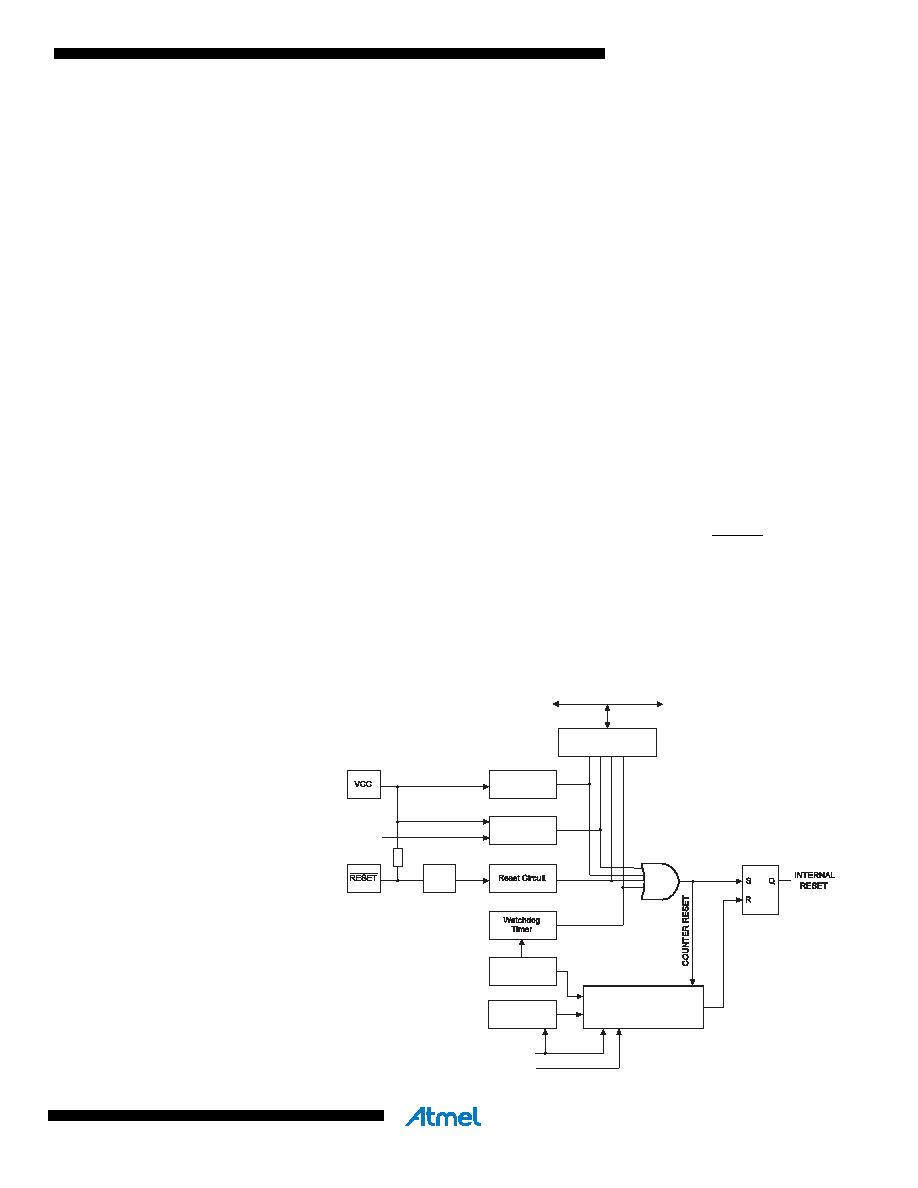
Vectors are in the Boot section or vice versa. The circuit diagram in Figure 9-1 shows the reset
logic. Table 9-1 defines the electrical parameters of the reset circuitry.
The I/O ports of the AVR are immediately reset to their initial state when a reset source goes
active. This does not require any clock source to be running.
After all reset sources have gone inactive, a delay counter is invoked, stretching the internal
reset. This allows the power to reach a stable level before normal operation starts. The time-out
period of the delay counter is defined by the user through the SUT and CKSEL Fuses. The dif-
ferent selections for the delay period are presented in “Clock Sources” on page 31.
9.0.2
Reset Sources
The AT90PWM2/2B/3/3B has four sources of reset:
Power-on Reset. The MCU is reset when the supply voltage is below the Power-on Reset
threshold (V
POT).
External Reset. The MCU is reset when a low level is present on the RESET pin for longer
than the minimum pulse length.
Watchdog Reset. The MCU is reset when the Watchdog Timer period expires and the
Watchdog is enabled.
Brown-out Reset. The MCU is reset when the supply voltage V
CC is below the Brown-out
Reset threshold (V
BOT) and the Brown-out Detector is enabled.
Figure 9-1.
Reset Logic
MCU Status
Register (MCUSR)
Brown-out
Reset Circuit
BODLEVEL [2..0]
Delay Counters
CKSEL[3:0]
CK
TIMEOUT
WDRF
BORF
EXTRF
PORF
DATA BUS
Clock
Generator
Spike
Filter
Pull-up Resistor
Watchdog
Oscillator
SUT[1:0]
Power-on Reset
Circuit
相关PDF资料 |
PDF描述 |
|---|---|
| EP20K100BC484-1 | LOADABLE PLD, PBGA484 |
| EP20K100BC484-2 | LOADABLE PLD, PBGA484 |
| EP20K100BC484-3 | LOADABLE PLD, PBGA484 |
| EP20K100BI484-1 | LOADABLE PLD, PBGA484 |
| EP20K100BI484-2 | LOADABLE PLD, PBGA484 |
相关代理商/技术参数 |
参数描述 |
|---|---|
| EP20K100BI356-1 | 制造商:未知厂家 制造商全称:未知厂家 功能描述:Field Programmable Gate Array (FPGA) |
| EP20K100BI356-1ES | 制造商:未知厂家 制造商全称:未知厂家 功能描述:FPGA |
| EP20K100BI356-2 | 制造商:未知厂家 制造商全称:未知厂家 功能描述:Field Programmable Gate Array (FPGA) |
| EP20K100BI356-2ES | 制造商:未知厂家 制造商全称:未知厂家 功能描述:FPGA |
| EP20K100BI356-3 | 制造商:未知厂家 制造商全称:未知厂家 功能描述:Field Programmable Gate Array (FPGA) |
发布紧急采购,3分钟左右您将得到回复。