参数资料
| 型号: | EP20K30EQC208-1 |
| 厂商: | Altera |
| 文件页数: | 47/117页 |
| 文件大小: | 0K |
| 描述: | IC APEX 20KE FPGA 300K 208-PQFP |
| 标准包装: | 24 |
| 系列: | APEX-20K® |
| LAB/CLB数: | 120 |
| 逻辑元件/单元数: | 1200 |
| RAM 位总计: | 24576 |
| 输入/输出数: | 125 |
| 门数: | 113000 |
| 电源电压: | 1.71 V ~ 1.89 V |
| 安装类型: | 表面贴装 |
| 工作温度: | 0°C ~ 85°C |
| 封装/外壳: | 208-BFQFP |
| 供应商设备封装: | 208-PQFP(28x28) |
第1页第2页第3页第4页第5页第6页第7页第8页第9页第10页第11页第12页第13页第14页第15页第16页第17页第18页第19页第20页第21页第22页第23页第24页第25页第26页第27页第28页第29页第30页第31页第32页第33页第34页第35页第36页第37页第38页第39页第40页第41页第42页第43页第44页第45页第46页当前第47页第48页第49页第50页第51页第52页第53页第54页第55页第56页第57页第58页第59页第60页第61页第62页第63页第64页第65页第66页第67页第68页第69页第70页第71页第72页第73页第74页第75页第76页第77页第78页第79页第80页第81页第82页第83页第84页第85页第86页第87页第88页第89页第90页第91页第92页第93页第94页第95页第96页第97页第98页第99页第100页第101页第102页第103页第104页第105页第106页第107页第108页第109页第110页第111页第112页第113页第114页第115页第116页第117页
Altera Corporation
35
APEX 20K Programmable Logic Device Family Data Sheet
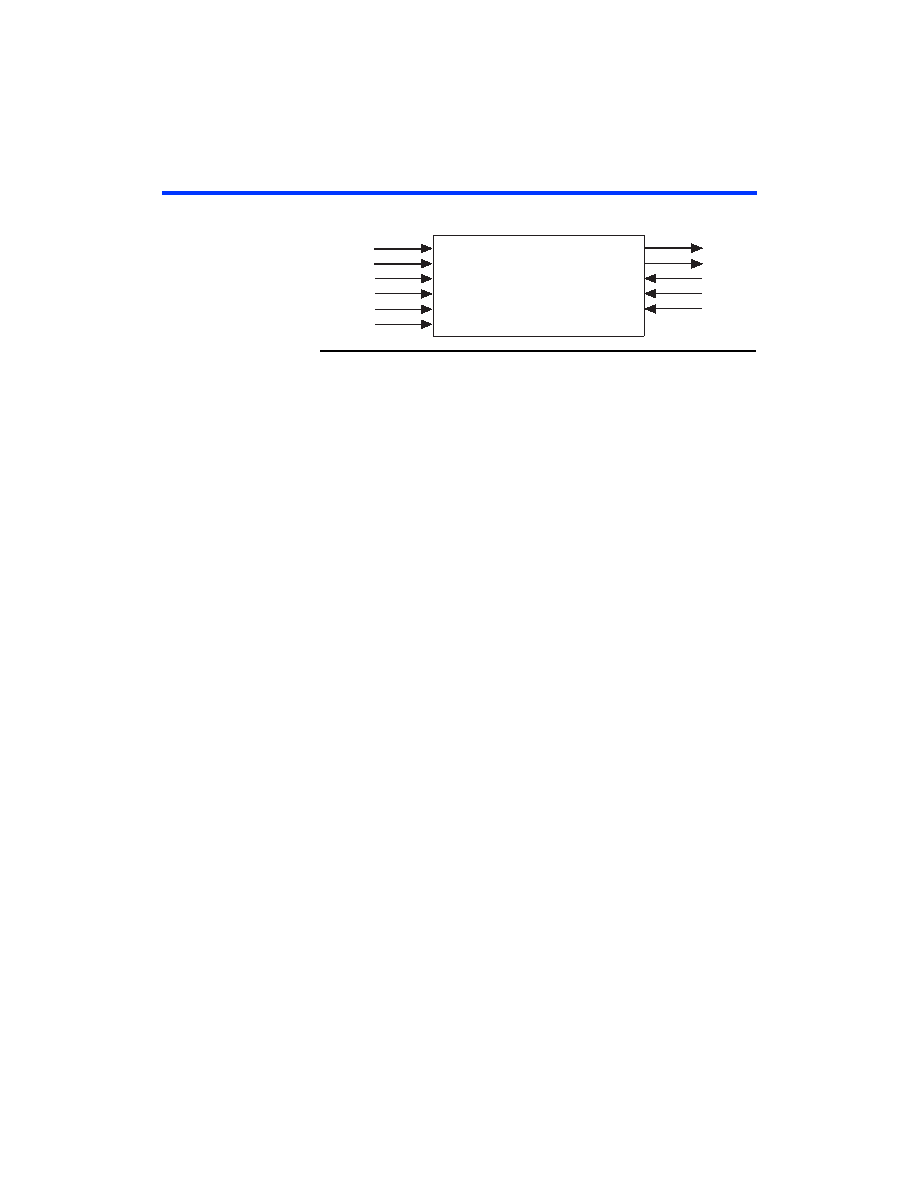
Figure 23. APEX 20KE CAM Block Diagram
CAM can be used in any application requiring high-speed searches, such
as networking, communications, data compression, and cache
management.
The APEX 20KE on-chip CAM provides faster system performance than
traditional discrete CAM. Integrating CAM and logic into the APEX 20KE
device eliminates off-chip and on-chip delays, improving system
performance.
When in CAM mode, the ESB implements 32-word, 32-bit CAM. Wider or
deeper CAM can be implemented by combining multiple CAMs with
some ancillary logic implemented in LEs. The Quartus II software
combines ESBs and LEs automatically to create larger CAMs.
CAM supports writing “don’t care” bits into words of the memory. The
“don’t-care” bit can be used as a mask for CAM comparisons; any bit set
to “don’t-care” has no effect on matches.
The output of the CAM can be encoded or unencoded. When encoded, the
ESB outputs an encoded address of the data’s location. For instance, if the
data is located in address 12, the ESB output is 12. When unencoded, the
ESB uses its 16 outputs to show the location of the data over two clock
cycles. In this case, if the data is located in address 12, the 12th output line
goes high. When using unencoded outputs, two clock cycles are required
to read the output because a 16-bit output bus is used to show the status
of 32 words.
The encoded output is better suited for designs that ensure duplicate data
is not written into the CAM. If duplicate data is written into two locations,
the CAM’s output will be incorrect. If the CAM may contain duplicate
data, the unencoded output is a better solution; CAM with unencoded
outputs can distinguish multiple data locations.
CAM can be pre-loaded with data during configuration, or it can be
written during system operation. In most cases, two clock cycles are
required to write each word into CAM. When “don’t-care” bits are used,
a third clock cycle is required.
wraddress[]
data[]
wren
inclock
inclocken
inaclr
data_address[]
match
outclock
outclocken
outaclr
相关PDF资料 |
PDF描述 |
|---|---|
| EP2AGX260FF35I3 | IC ARRIA II GX 260K 1152FBGA |
| EP2S130F1508I5 | IC STRATIX II FPGA 130K 1508FBGA |
| EP2SGX90FF1508C5ES | IC STRATIX II GX 90K 1508-FBGA |
| EP3SL340F1760C3N | IC STRATIX III L 340K 1760-FBGA |
| EP4CGX150DF31I7 | IC CYCLONE IV FPGA 150K 896FBGA |
相关代理商/技术参数 |
参数描述 |
|---|---|
| EP20K30EQC208-1ES | 制造商:未知厂家 制造商全称:未知厂家 功能描述:FPGA |
| EP20K30EQC208-2 | 制造商:Rochester Electronics LLC 功能描述:- Bulk |
| EP20K30EQC208-2ES | 制造商:未知厂家 制造商全称:未知厂家 功能描述:FPGA |
| EP20K30EQC208-3 | 制造商:Rochester Electronics LLC 功能描述:- Bulk |
| EP20K30EQC208-3ES | 制造商:未知厂家 制造商全称:未知厂家 功能描述:FPGA |
发布紧急采购,3分钟左右您将得到回复。