参数资料
| 型号: | EP20K30EQC208-1 |
| 厂商: | Altera |
| 文件页数: | 68/117页 |
| 文件大小: | 0K |
| 描述: | IC APEX 20KE FPGA 300K 208-PQFP |
| 标准包装: | 24 |
| 系列: | APEX-20K® |
| LAB/CLB数: | 120 |
| 逻辑元件/单元数: | 1200 |
| RAM 位总计: | 24576 |
| 输入/输出数: | 125 |
| 门数: | 113000 |
| 电源电压: | 1.71 V ~ 1.89 V |
| 安装类型: | 表面贴装 |
| 工作温度: | 0°C ~ 85°C |
| 封装/外壳: | 208-BFQFP |
| 供应商设备封装: | 208-PQFP(28x28) |
第1页第2页第3页第4页第5页第6页第7页第8页第9页第10页第11页第12页第13页第14页第15页第16页第17页第18页第19页第20页第21页第22页第23页第24页第25页第26页第27页第28页第29页第30页第31页第32页第33页第34页第35页第36页第37页第38页第39页第40页第41页第42页第43页第44页第45页第46页第47页第48页第49页第50页第51页第52页第53页第54页第55页第56页第57页第58页第59页第60页第61页第62页第63页第64页第65页第66页第67页当前第68页第69页第70页第71页第72页第73页第74页第75页第76页第77页第78页第79页第80页第81页第82页第83页第84页第85页第86页第87页第88页第89页第90页第91页第92页第93页第94页第95页第96页第97页第98页第99页第100页第101页第102页第103页第104页第105页第106页第107页第108页第109页第110页第111页第112页第113页第114页第115页第116页第117页
54
Altera Corporation
APEX 20K Programmable Logic Device Family Data Sheet
(1)
All input clock specifications must be met. The PLL may not lock onto an incoming clock if the clock specifications
are not met, creating an erroneous clock within the device.
(2)
The maximum lock time is 40 s or 2000 input clock cycles, whichever occurs first.
(3)
Before configuration, the PLL circuits are disable and powered down. During configuration, the PLLs are still
disabled. The PLLs begin to lock once the device is in the user mode. If the clock enable feature is used, lock begins
once the CLKLK_ENA pin goes high in user mode.
(4)
The PLL VCO operating range is 200 MHz fVCO 840 MHz for LVDS mode.
SignalTap
Embedded
Logic Analyzer
APEX 20K devices include device enhancements to support the SignalTap
embedded logic analyzer. By including this circuitry, the APEX 20K
device provides the ability to monitor design operation over a period of
time through the IEEE Std. 1149.1 (JTAG) circuitry; a designer can analyze
internal logic at speed without bringing internal signals to the I/O pins.
This feature is particularly important for advanced packages such as
FineLine BGA packages because adding a connection to a pin during the
debugging process can be difficult after a board is designed and
manufactured.
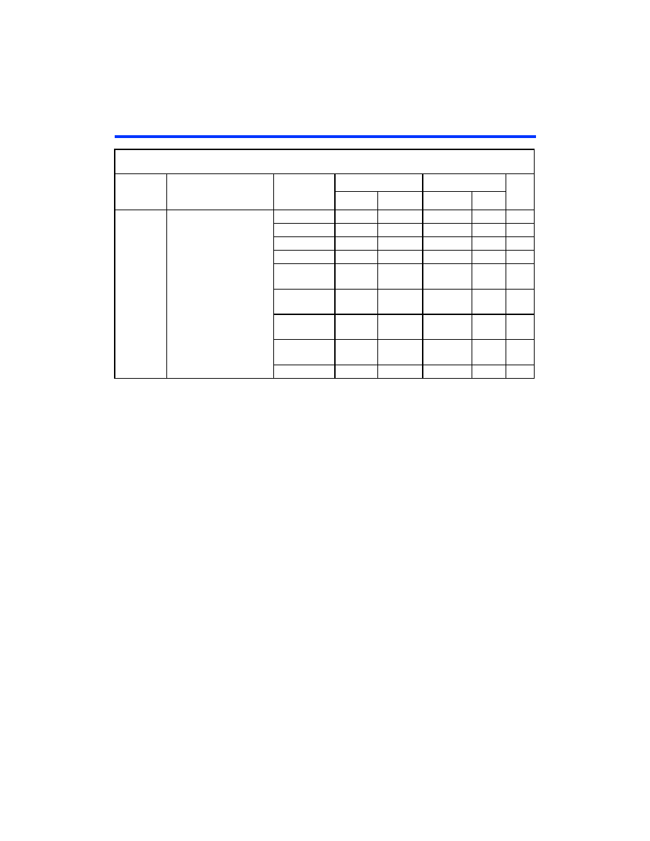
fIN
Input clock frequency
3.3-V LVTTL
1.5
290
1.5
257
MHz
2.5-V LVTTL
1.5
281
1.5
250
MHz
1.8-V LVTTL
1.5
272
1.5
243
MHz
GTL+
1.5
303
1.5
261
MHz
SSTL-2 Class
I
1.5
291
1.5
253
MHz
SSTL-2 Class
II
1.5
291
1.5
253
MHz
SSTL-3 Class
I
1.5
300
1.5
260
MHz
SSTL-3 Class
II
1.5
300
1.5
260
MHz
LVDS
1.5
420
1.5
350
MHz
Table 18. APEX 20KE Clock Input & Output Parameters
(Part 2 of 2)
Note (1)
Symbol
Parameter
I/O Standard
-1X Speed Grade
-2X Speed Grade
Units
Min
Max
Min
Max
相关PDF资料 |
PDF描述 |
|---|---|
| EP2AGX260FF35I3 | IC ARRIA II GX 260K 1152FBGA |
| EP2S130F1508I5 | IC STRATIX II FPGA 130K 1508FBGA |
| EP2SGX90FF1508C5ES | IC STRATIX II GX 90K 1508-FBGA |
| EP3SL340F1760C3N | IC STRATIX III L 340K 1760-FBGA |
| EP4CGX150DF31I7 | IC CYCLONE IV FPGA 150K 896FBGA |
相关代理商/技术参数 |
参数描述 |
|---|---|
| EP20K30EQC208-1ES | 制造商:未知厂家 制造商全称:未知厂家 功能描述:FPGA |
| EP20K30EQC208-2 | 制造商:Rochester Electronics LLC 功能描述:- Bulk |
| EP20K30EQC208-2ES | 制造商:未知厂家 制造商全称:未知厂家 功能描述:FPGA |
| EP20K30EQC208-3 | 制造商:Rochester Electronics LLC 功能描述:- Bulk |
| EP20K30EQC208-3ES | 制造商:未知厂家 制造商全称:未知厂家 功能描述:FPGA |
发布紧急采购,3分钟左右您将得到回复。