参数资料
| 型号: | EP2AGX65DF29C6N |
| 厂商: | Altera |
| 文件页数: | 15/90页 |
| 文件大小: | 0K |
| 描述: | IC ARRIA II GX FPGA 65K 780FBGA |
| 产品培训模块: | Three Reasons to Use FPGA's in Industrial Designs |
| 标准包装: | 4 |
| 系列: | Arria II GX |
| LAB/CLB数: | 2530 |
| 逻辑元件/单元数: | 60214 |
| RAM 位总计: | 5371904 |
| 输入/输出数: | 364 |
| 电源电压: | 0.87 V ~ 0.93 V |
| 安装类型: | 表面贴装 |
| 工作温度: | 0°C ~ 85°C |
| 封装/外壳: | 780-BBGA |
| 供应商设备封装: | 780-FBGA(29x29) |
第1页第2页第3页第4页第5页第6页第7页第8页第9页第10页第11页第12页第13页第14页当前第15页第16页第17页第18页第19页第20页第21页第22页第23页第24页第25页第26页第27页第28页第29页第30页第31页第32页第33页第34页第35页第36页第37页第38页第39页第40页第41页第42页第43页第44页第45页第46页第47页第48页第49页第50页第51页第52页第53页第54页第55页第56页第57页第58页第59页第60页第61页第62页第63页第64页第65页第66页第67页第68页第69页第70页第71页第72页第73页第74页第75页第76页第77页第78页第79页第80页第81页第82页第83页第84页第85页第86页第87页第88页第89页第90页
1–14
Chapter 1: Device Datasheet for Arria II Devices
Electrical Characteristics
December 2013
Altera Corporation
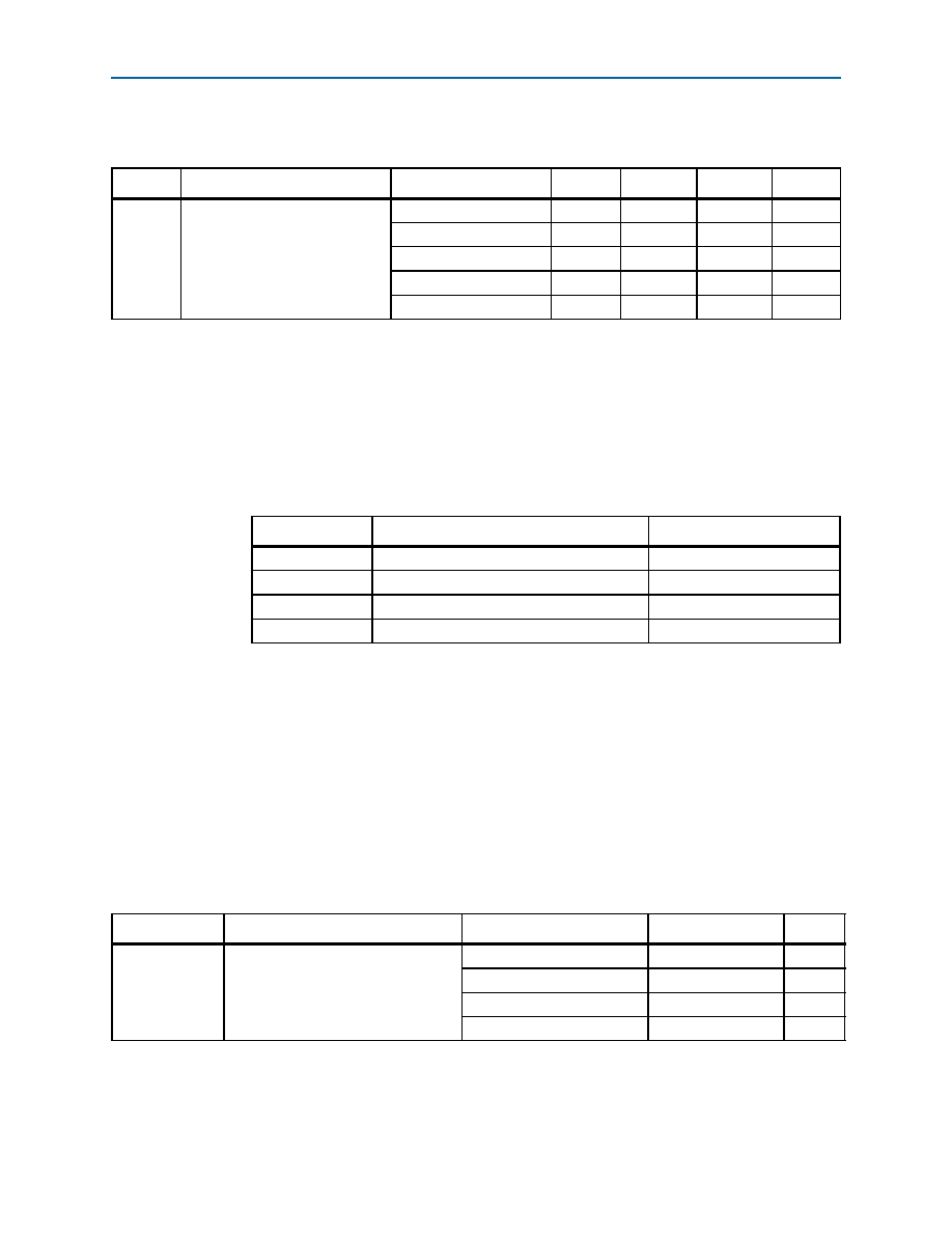
Table 1–19 lists the weak pull-up resistor values for Arria II GZ devices.
Hot Socketing
Table 1–20 lists the hot-socketing specification for Arria II GX and GZ devices.
Schmitt Trigger Input
The Arria II GX device supports Schmitt trigger input on the TDI, TMS, TCK, nSTATUS,
nCONFIG
, nCE, CONF_DONE, and DCLK pins. A Schmitt trigger feature introduces
hysteresis to the input signal for improved noise immunity, especially for signals with
slow edge rates.
Schmitt trigger inputs in Arria II GX devices.
Table 1–19. Internal Weak Pull-Up Resistor for Arria II GZ Devices
Symbol
Description
Conditions
Min
Typ
Max
Unit
RPU
Value of the I/O pin pull-up
resistor before and during
configuration, as well as user
mode if the programmable
pull-up resistor option is enabled.
—25
—
k
—25
—
k
—25
—
k
—25
—
k
—25
—
k
Notes to Table 1–19:
(1) All I/O pins have an option to enable weak pull-up except configuration, test, and JTAG pins.
(2) The internal weak pull-down feature is only available for the JTAG TCK pin. The typical value for this internal weak pull-down resistor is
approximately 25 k
(3) Pin pull-up resistance values may be lower if an external source drives the pin higher than VCCIO.
Table 1–20. Hot Socketing Specifications for Arria II Devices
Symbol
Description
Maximum
IIIOPIN(DC)
DC current per I/O pin
300
A
IIOPIN(AC)
AC current per I/O pin
8 mA (1)
IXCVRTX(DC)
DC current per transceiver TX pin
100 mA
IXCVRRX(DC)
DC current per transceiver RX pin
50 mA
Note to Table 1–20:
(1) The I/O ramp rate is 10 ns or more. For ramp rates faster than 10 ns, |IIOPIN| = C dv/dt, in which “C” is I/O pin
capacitance and “dv/dt” is slew rate.
Table 1–21. Schmitt Trigger Input Hysteresis Specifications for Arria II GX Devices
Symbol
Description
Condition (V)
Minimum
Unit
VSchmitt
Hysteresis for Schmitt trigger input
VCCIO = 3.3
220
mV
VCCIO = 2.5
180
mV
VCCIO = 1.8
110
mV
VCCIO = 1.5
70
mV
相关PDF资料 |
PDF描述 |
|---|---|
| RMC49DRAS-S734 | CONN EDGECARD 98POS .100 R/A PCB |
| A42MX36-3PQ240I | IC FPGA MX SGL CHIP 54K 240-PQFP |
| GBB108DHAR | CONN EDGECARD 216PS R/A .050 SLD |
| A42MX36-3PQG240I | IC FPGA MX SGL CHIP 54K 240-PQFP |
| EP1S10F780I6 | IC STRATIX FPGA 10K LE 780-FBGA |
相关代理商/技术参数 |
参数描述 |
|---|---|
| EP2AGX65DF29C6NES | 制造商:Altera Corporation 功能描述:FPGA Arria |
| EP2AGX65DF29I3 | 功能描述:IC ARRIA II GX FPGA 65K 780FBGA RoHS:否 类别:集成电路 (IC) >> 嵌入式 - FPGA(现场可编程门阵列) 系列:Arria II GX 产品变化通告:XC4000(E,L) Discontinuation 01/April/2002 标准包装:24 系列:XC4000E/X LAB/CLB数:100 逻辑元件/单元数:238 RAM 位总计:3200 输入/输出数:80 门数:3000 电源电压:4.5 V ~ 5.5 V 安装类型:表面贴装 工作温度:-40°C ~ 100°C 封装/外壳:120-BCBGA 供应商设备封装:120-CPGA(34.55x34.55) |
| EP2AGX65DF29I3N | 功能描述:FPGA - 现场可编程门阵列 FPGA - Arria II GX 2530 LABs 364 IOs RoHS:否 制造商:Altera Corporation 系列:Cyclone V E 栅极数量: 逻辑块数量:943 内嵌式块RAM - EBR:1956 kbit 输入/输出端数量:128 最大工作频率:800 MHz 工作电源电压:1.1 V 最大工作温度:+ 70 C 安装风格:SMD/SMT 封装 / 箱体:FBGA-256 |
| EP2AGX65DF29I5 | 功能描述:FPGA - 现场可编程门阵列 FPGA - Arria II GX 2530 LABs 364 IOs RoHS:否 制造商:Altera Corporation 系列:Cyclone V E 栅极数量: 逻辑块数量:943 内嵌式块RAM - EBR:1956 kbit 输入/输出端数量:128 最大工作频率:800 MHz 工作电源电压:1.1 V 最大工作温度:+ 70 C 安装风格:SMD/SMT 封装 / 箱体:FBGA-256 |
| EP2AGX65DF29I5N | 功能描述:FPGA - 现场可编程门阵列 FPGA - Arria II GX 2530 LABs 364 IOs RoHS:否 制造商:Altera Corporation 系列:Cyclone V E 栅极数量: 逻辑块数量:943 内嵌式块RAM - EBR:1956 kbit 输入/输出端数量:128 最大工作频率:800 MHz 工作电源电压:1.1 V 最大工作温度:+ 70 C 安装风格:SMD/SMT 封装 / 箱体:FBGA-256 |
发布紧急采购,3分钟左右您将得到回复。