参数资料
| 型号: | EP2AGX65DF29C6N |
| 厂商: | Altera |
| 文件页数: | 72/90页 |
| 文件大小: | 0K |
| 描述: | IC ARRIA II GX FPGA 65K 780FBGA |
| 产品培训模块: | Three Reasons to Use FPGA's in Industrial Designs |
| 标准包装: | 4 |
| 系列: | Arria II GX |
| LAB/CLB数: | 2530 |
| 逻辑元件/单元数: | 60214 |
| RAM 位总计: | 5371904 |
| 输入/输出数: | 364 |
| 电源电压: | 0.87 V ~ 0.93 V |
| 安装类型: | 表面贴装 |
| 工作温度: | 0°C ~ 85°C |
| 封装/外壳: | 780-BBGA |
| 供应商设备封装: | 780-FBGA(29x29) |
第1页第2页第3页第4页第5页第6页第7页第8页第9页第10页第11页第12页第13页第14页第15页第16页第17页第18页第19页第20页第21页第22页第23页第24页第25页第26页第27页第28页第29页第30页第31页第32页第33页第34页第35页第36页第37页第38页第39页第40页第41页第42页第43页第44页第45页第46页第47页第48页第49页第50页第51页第52页第53页第54页第55页第56页第57页第58页第59页第60页第61页第62页第63页第64页第65页第66页第67页第68页第69页第70页第71页当前第72页第73页第74页第75页第76页第77页第78页第79页第80页第81页第82页第83页第84页第85页第86页第87页第88页第89页第90页
1–66
Chapter 1: Device Datasheet for Arria II Devices
Switching Characteristics
December 2013
Altera Corporation
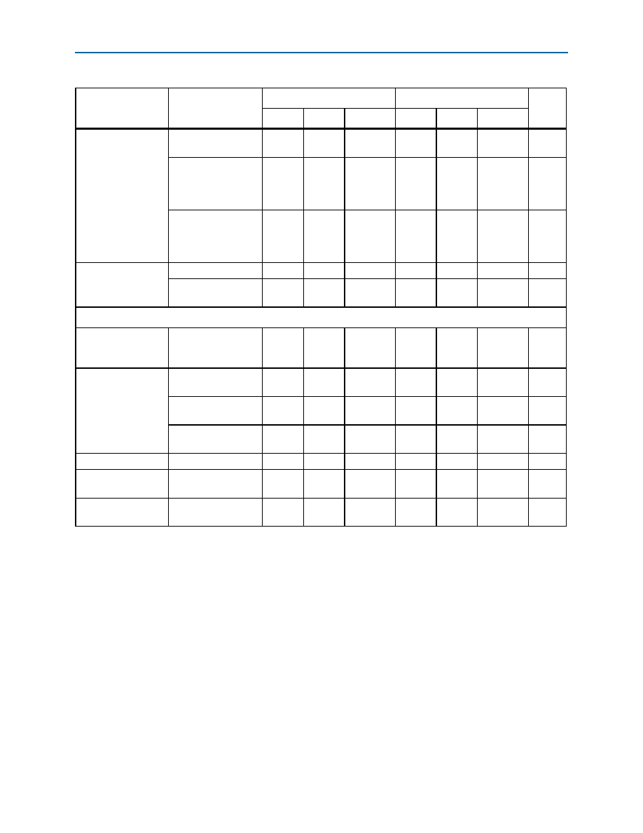
Table 1–55 lists DPA lock time specifications for Arria II GX and GZ devices.
tRISE & tFALL
True differential I/O
standards
—
200—
—200
ps
Emulated differential
I/O standards with
three external output
resistor networks
—
250—
—300
ps
Emulated differential
I/O standards with
one external output
resistor
—
500—
—500
ps
TCCS
True LVDS
—
100
—
100
ps
Emulated
LVDS_E_3R
—
250—
—250
ps
Receiver
True differential I/O
standards - fHSDRDPA
(data rate)
SERDES factor
J = 3 to 10
150
—
1250
150
—
1250
Mbps
fHSDR (data rate)
SERDES factor
J = 3 to 10
—
—
Mbps
SERDES factor J = 2,
uses DDR registers
—
—
Mbps
SERDES factor J = 1,
uses an SDR register
—
—
Mbps
DPA run length
DPA mode
—
10000
—
10000
UI
Soft-CDR PPM
tolerance
Soft-CDR mode
—
300
—
300
± PPM
Sampling Window
(SW)
Non-DPA mode
—
300
—
300
ps
Notes to Table 1–54:
(1) When J = 3 to 10, use the SERDES block.
(2) When J = 1 or 2, bypass the SERDES block.
(3) Clock Boost Factor (W) is the ratio between input data rate to the input clock rate.
(4) The minimum specification depends on the clock source (for example, the PLL and clock pin) and the clock routing resource (global, regional,
or local) that you use. The I/O differential buffer and input register do not have a minimum toggle rate.
(5) You must calculate the leftover timing margin in the receiver by performing link timing closure analysis. You must consider the board skew
margin, transmitter channel-to-channel skew, and receiver sampling margin to determine leftover timing margin.
(6) You can estimate the achievable maximum data rate for non-DPA mode by performing link timing closure analysis. You must consider the board
skew margin, transmitter delay margin, and the receiver sampling margin to determine the maximum data rate supported.
(7) This is achieved by using the LVDS and DPA clock network.
(8) If the receiver with DPA enabled and transmitter are using shared PLLs, the minimum data rate is 150 Mbps.
(9) This only applies to DPA and soft-CDR modes.
(10) This only applies to LVDS source synchronous mode.
Table 1–54. High-Speed I/O Specifications for Arria II GZ Devices (Note 1), (2), (10) (Part 3 of 3)
Symbol
Conditions
C3, I3
C4, I4
Unit
Min
Typ
Max
Min
Typ
Max
相关PDF资料 |
PDF描述 |
|---|---|
| RMC49DRAS-S734 | CONN EDGECARD 98POS .100 R/A PCB |
| A42MX36-3PQ240I | IC FPGA MX SGL CHIP 54K 240-PQFP |
| GBB108DHAR | CONN EDGECARD 216PS R/A .050 SLD |
| A42MX36-3PQG240I | IC FPGA MX SGL CHIP 54K 240-PQFP |
| EP1S10F780I6 | IC STRATIX FPGA 10K LE 780-FBGA |
相关代理商/技术参数 |
参数描述 |
|---|---|
| EP2AGX65DF29C6NES | 制造商:Altera Corporation 功能描述:FPGA Arria |
| EP2AGX65DF29I3 | 功能描述:IC ARRIA II GX FPGA 65K 780FBGA RoHS:否 类别:集成电路 (IC) >> 嵌入式 - FPGA(现场可编程门阵列) 系列:Arria II GX 产品变化通告:XC4000(E,L) Discontinuation 01/April/2002 标准包装:24 系列:XC4000E/X LAB/CLB数:100 逻辑元件/单元数:238 RAM 位总计:3200 输入/输出数:80 门数:3000 电源电压:4.5 V ~ 5.5 V 安装类型:表面贴装 工作温度:-40°C ~ 100°C 封装/外壳:120-BCBGA 供应商设备封装:120-CPGA(34.55x34.55) |
| EP2AGX65DF29I3N | 功能描述:FPGA - 现场可编程门阵列 FPGA - Arria II GX 2530 LABs 364 IOs RoHS:否 制造商:Altera Corporation 系列:Cyclone V E 栅极数量: 逻辑块数量:943 内嵌式块RAM - EBR:1956 kbit 输入/输出端数量:128 最大工作频率:800 MHz 工作电源电压:1.1 V 最大工作温度:+ 70 C 安装风格:SMD/SMT 封装 / 箱体:FBGA-256 |
| EP2AGX65DF29I5 | 功能描述:FPGA - 现场可编程门阵列 FPGA - Arria II GX 2530 LABs 364 IOs RoHS:否 制造商:Altera Corporation 系列:Cyclone V E 栅极数量: 逻辑块数量:943 内嵌式块RAM - EBR:1956 kbit 输入/输出端数量:128 最大工作频率:800 MHz 工作电源电压:1.1 V 最大工作温度:+ 70 C 安装风格:SMD/SMT 封装 / 箱体:FBGA-256 |
| EP2AGX65DF29I5N | 功能描述:FPGA - 现场可编程门阵列 FPGA - Arria II GX 2530 LABs 364 IOs RoHS:否 制造商:Altera Corporation 系列:Cyclone V E 栅极数量: 逻辑块数量:943 内嵌式块RAM - EBR:1956 kbit 输入/输出端数量:128 最大工作频率:800 MHz 工作电源电压:1.1 V 最大工作温度:+ 70 C 安装风格:SMD/SMT 封装 / 箱体:FBGA-256 |
发布紧急采购,3分钟左右您将得到回复。